ADSP-3PARCBF548E02 Analog Devices Inc, ADSP-3PARCBF548E02 Datasheet - Page 34
ADSP-3PARCBF548E02
Manufacturer Part Number
ADSP-3PARCBF548E02
Description
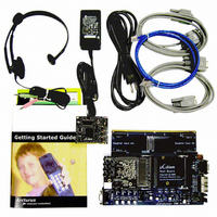
KIT DEV STARTER BF548
Manufacturer
Analog Devices Inc
Series
Blackfin®r
Type
DSPr
Specifications of ADSP-3PARCBF548E02
Contents
Board, Cables, CD, Headset with Microphone, Module, Power Supply
For Use With/related Products
ADSP-BF548
Lead Free Status / RoHS Status
Lead free / RoHS Compliant


ADSP-BF542/ADSP-BF544/ADSP-BF547/ADSP-BF548/ADSP-BF549
SPECIFICATIONS
Component specifications are subject to change without notice.
OPERATING CONDITIONS
1
2
3
4
5
6
Parameter
V
V
V
V
V
V
V
V
V
V
V
V
V
V
V
V
V
T
See
V
V
Use of the internal voltage regulator is not supported on 600 MHz speed grade models or on automotive grade models. An external voltage regulator must be used.
Bidirectional pins (D15–0, PA15–0, PB14–0, PC15–0, PD15–0, PE15–0, PF15–0, PG15–0, PH13–0, PI15–0, PJ14–0) and input pins (ATAPI_PDIAG, USB_ID, TCK, TDI,
Parameter value applies to all input and bidirectional pins except PB1-0, PE15-14, PG15–11, PH7-6, DQ0-15, and DQS0-1.
TMS, TRST, CLKIN, RESET, NMI, and BMODE3–0) of the ADSP-BF54x Blackfin processors are 3.3 V-tolerant (always accept up to 3.6 V maximum V
compliance (on outputs, V
J
DDINT
DDEXT
DDUSB
DDMP
DDRTC
DDDDR
DDVR
IH
IHDDR
IH5V
IHTWI
IHUSB
IL
IL5V
ILDDR
ILTWI
DDR_VREF
DDINT
DDEXT
14
Table 13 on Page 35
12
4
1, 2
3
maximum is 1.10 V during one-time-programmable (OTP) memory programming operations.
minimum is 3.0 V and maximum is 3.6 V during OTP memory programming operations.
Internal Supply Voltage
Internal Supply Voltage
Internal Supply Voltage
External Supply Voltage
External Supply Voltage
External Supply Voltage
USB External Supply Voltage
MXVR PLL Supply Voltage
MXVR PLL Supply Voltage
Real Time Clock Supply Voltage
Real Time Clock Supply Voltage
DDR Memory Supply Voltage
DDR Memory Supply Voltage
Internal Voltage Regulator
Supply Voltage
High Level Input Voltage
High Level Input Voltage
High Level Input Voltage
High Level Input Voltage
High Level Input Voltage
High Level Input Voltage
Low Level Input Voltage
Low Level Input Voltage
Low Level Input Voltage
Low Level Input Voltage
Low Level Input Voltage
Low Level Input Voltage
DDR_VREF Pin Input Voltage
Junction Temperature
(400/533 MHz)
Junction Temperature (600 MHz) 400-Ball Chip Scale Package Ball
for frequency/voltage specifications.
OH
) is limited by the V
5, 11
12
12
7
7
9, 13
5, 6
7
7
8
10
9, 13
DDEXT
supply voltage. The regulator can generate V
Conditions
Nonautomotive grade models
Automotive grade models
Mobile DDR SDRAM models
Nonautomotive 3.3 V I/O
Nonautomotive 2.5 V I/O
Automotive grade models
Nonautomotive grade models
Automotive grade models
Nonautomotive grade models
Automotive grade models
DDR SDRAM models
Mobile DDR SDRAM models
V
DDR SDRAM models
Mobile DDR SDRAM models
V
V
V
3.3 V I/O, V
2.5 V I/O, V
DDR SDRAM models
Mobile DDR SDRAM models
400-Ball Chip Scale Package Ball
Grid Array (CSP_BGA) @T
–40
Grid Array (CSP_BGA) @T
0
Rev. C | Page 34 of 100 | February 2010
º
DDEXT
DDEXT
DDEXT
DDEXT
C to +70
º
C to +85
= maximum
= maximum
= maximum
= minimum
º
DDEXT
DDEXT
C
º
C
= minimum
= minimum
AMBIENT
AMBIENT
=
=
DDINT
V
V
DDR_VREF
at levels of 0.90 V to 1.30 V with -5% to +5% tolerance.
0.49 x V
DDR_VREF
0.7 x V
1.14
2.25
2.25
–0.3
–0.3
–0.3
–0.3
–0.3
–0.3
Min
–40
0.9
1.0
2.7
2.7
3.0
0.9
1.0
2.7
2.5
1.8
2.7
2.0
2.0
0
+ 0.125
DDEXT
+ 0.15
DDDDR
Nominal
V
0.50 x
1.875
DDDDR
3.3
2.5
3.3
3.3
3.3
2.6
3.3
V
V
DDR_VREF
0.51 x V
V
V
DDR_VREF
0.3 x V
DDDDR
DDDDR
+105
Max
2.75
1.43
1.38
1.31
1.43
1.38
1.95
5.25
+90
3.6
3.6
3.6
3.6
3.6
2.7
3.6
3.6
5.5
5.5
0.6
0.8
0.6
– 0.125 V
+ 0.3
+ 0.3
DDEXT
– 0.15 V
DDDDR
IH
). Voltage
V
V
V
V
V
V
V
V
V
V
V
V
V
V
V
V
V
V
V
V
V
V
V
V
º
º
Unit
V
C
C
Related parts for ADSP-3PARCBF548E02
Image
Part Number
Description
Manufacturer
Datasheet
Request
R

Part Number:
Description:
±1.7g Dual-Axis IMEMS Accelerometer Evaluation Board
Manufacturer:
Analog Devices Inc
Datasheet:

Part Number:
Description:
Inertial Sensor Evaluation System
Manufacturer:
Analog Devices Inc
Datasheet:
Part Number:
Description:
Manufacturer:
Analog Devices Inc
Datasheet:
Part Number:
Description:
Manufacturer:
Analog Devices Inc
Datasheet:
Part Number:
Description:
Manufacturer:
Analog Devices Inc
Datasheet:
Part Number:
Description:
Manufacturer:
Analog Devices Inc
Datasheet:
Part Number:
Description:
Manufacturer:
Analog Devices Inc
Datasheet:
Part Number:
Description:
Manufacturer:
Analog Devices Inc
Datasheet:
Part Number:
Description:
Manufacturer:
Analog Devices Inc
Datasheet:
Part Number:
Description:
Manufacturer:
Analog Devices Inc
Datasheet:
Part Number:
Description:
Manufacturer:
Analog Devices Inc
Datasheet:
Part Number:
Description:
Manufacturer:
Analog Devices Inc
Datasheet:
Part Number:
Description:
Manufacturer:
Analog Devices Inc
Datasheet: