C8051F411EK Silicon Laboratories Inc, C8051F411EK Datasheet - Page 143
C8051F411EK
Manufacturer Part Number
C8051F411EK
Description
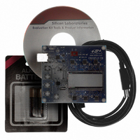
KIT EVAL FOR C8051F411
Manufacturer
Silicon Laboratories Inc
Type
MCUr
Specifications of C8051F411EK
Contents
Evaluation Board, CD-ROM, USB Cable, Batteries and User Guide
Processor To Be Evaluated
C8051F41x
Interface Type
USB
Silicon Manufacturer
Silicon Labs
Core Architecture
8051
Silicon Core Number
C8051F411
Silicon Family Name
C8051F41x
Kit Contents
LCD Based Evaluation Board, USB Cable, Software CD And Quick-Start Guide
Lead Free Status / RoHS Status
Contains lead / RoHS non-compliant
For Use With/related Products
Silicon Laboratories C8051F41x
For Use With
336-1315 - KIT REF DESIGN VOICE RECORD F41X
Lead Free Status / Rohs Status
Lead free / RoHS Compliant
Other names
336-1317


Table 16.2. Flash Electrical Characteristics
V
Flash Size
Endurance
Erase Cycle Time
Write Cycle Time
Read Cycle Time
V
*Note: 512 bytes at addresses 0x7E00 to 0x7FFF are reserved.
DD
DD
Bits7–4: UNUSED. Read = 0000b. Write = don’t care.
Bits3–0: PERIOD: Oneshot Period Control Bits.
= 2.0 to 2.75 V; –40 to +85 ºC unless otherwise specified. Typical values are given at 25 ºC.
Bit7
Parameter
R
-
These bits limit the internal Flash read strobe width as follows. When the Flash read strobe
is de-asserted, the Flash memory enters a low-power state for the remainder of the system
clock cycle. These bits have no effect when the system clocks is greater than 12.5 MHz and
FLRT = 0.
FLASH
Bit6
SFR Definition 16.4. ONESHOT: Flash Oneshot Period
R
-
RDMAX
C8051F410/1
C8051F412/3
V
FLSCL.3–0 written to '0000'
FLSCL.3–0 written to '0000'
Write/Erase Operations
DD
Bit5
is 2.2 V or greater
R
-
=
5ns
Conditions
+
Bit4
R
-
PERIOD 5ns
Rev. 1.1
R/W
Bit3
32768*
16384
2.25
20 k
Min
R/W
Bit2
16
38
40
PERIOD
C8051F410/1/2/3
90 k
Typ
20
46
—
—
—
R/W
Bit1
SFR Address:
Max
57
—
—
24
—
—
R/W
Bit0
Erase/Write
0xAF
Reset Value
00001111
Units
bytes
ms
µs
ns
V
143
Related parts for C8051F411EK
Image
Part Number
Description
Manufacturer
Datasheet
Request
R

Part Number:
Description:
SMD/C°/SINGLE-ENDED OUTPUT SILICON OSCILLATOR
Manufacturer:
Silicon Laboratories Inc
Part Number:
Description:
Manufacturer:
Silicon Laboratories Inc
Datasheet:
Part Number:
Description:
N/A N/A/SI4010 AES KEYFOB DEMO WITH LCD RX
Manufacturer:
Silicon Laboratories Inc
Datasheet:
Part Number:
Description:
N/A N/A/SI4010 SIMPLIFIED KEY FOB DEMO WITH LED RX
Manufacturer:
Silicon Laboratories Inc
Datasheet:
Part Number:
Description:
N/A/-40 TO 85 OC/EZLINK MODULE; F930/4432 HIGH BAND (REV E/B1)
Manufacturer:
Silicon Laboratories Inc
Part Number:
Description:
EZLink Module; F930/4432 Low Band (rev e/B1)
Manufacturer:
Silicon Laboratories Inc
Part Number:
Description:
I°/4460 10 DBM RADIO TEST CARD 434 MHZ
Manufacturer:
Silicon Laboratories Inc
Part Number:
Description:
I°/4461 14 DBM RADIO TEST CARD 868 MHZ
Manufacturer:
Silicon Laboratories Inc
Part Number:
Description:
I°/4463 20 DBM RFSWITCH RADIO TEST CARD 460 MHZ
Manufacturer:
Silicon Laboratories Inc
Part Number:
Description:
I°/4463 20 DBM RADIO TEST CARD 868 MHZ
Manufacturer:
Silicon Laboratories Inc
Part Number:
Description:
I°/4463 27 DBM RADIO TEST CARD 868 MHZ
Manufacturer:
Silicon Laboratories Inc
Part Number:
Description:
I°/4463 SKYWORKS 30 DBM RADIO TEST CARD 915 MHZ
Manufacturer:
Silicon Laboratories Inc
Part Number:
Description:
N/A N/A/-40 TO 85 OC/4463 RFMD 30 DBM RADIO TEST CARD 915 MHZ
Manufacturer:
Silicon Laboratories Inc
Part Number:
Description:
I°/4463 20 DBM RADIO TEST CARD 169 MHZ
Manufacturer:
Silicon Laboratories Inc