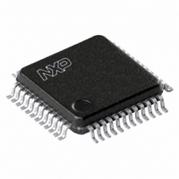
LPC1114FBD48/301,1 NXP Semiconductors, LPC1114FBD48/301,1 Datasheet - Page 12

LPC1114FBD48/301,1
Manufacturer Part Number
LPC1114FBD48/301,1
Description
IC MCU 32BIT 32KB FLASH 48LQFP
Manufacturer
NXP Semiconductors
Series
LPC1100r
Datasheets
1.LPC1114FHN333015.pdf
(2 pages)
2.LPC1114FHN333015.pdf
(66 pages)
3.LPC1114FHN333015.pdf
(66 pages)
Specifications of LPC1114FBD48/301,1
Program Memory Type
FLASH
Program Memory Size
32KB (32K x 8)
Package / Case
48-LQFP
Core Processor
ARM Cortex-M0
Core Size
32-Bit
Speed
50MHz
Connectivity
I²C, SPI, UART/USART
Peripherals
Brown-out Detect/Reset, POR, WDT
Number Of I /o
42
Ram Size
8K x 8
Voltage - Supply (vcc/vdd)
1.8 V ~ 3.6 V
Data Converters
A/D 8x10b
Oscillator Type
Internal
Operating Temperature
-40°C ~ 85°C
Processor Series
LPC11
Core
ARM Cortex M0
Data Bus Width
32 bit
Data Ram Size
8 KB
Interface Type
I2C, SPI, UART
Number Of Programmable I/os
28
Operating Supply Voltage
1.8 V to 3.6 V
Maximum Operating Temperature
+ 85 C
Mounting Style
SMD/SMT
3rd Party Development Tools
MDK-ARM, RL-ARM, ULINK2, KSK-LPC1114
Development Tools By Supplier
OM11049, OM11085
Minimum Operating Temperature
- 40 C
On-chip Adc
10 bit, 8 Channel
Lead Free Status / RoHS Status
Lead free / RoHS Compliant
For Use With
622-1005 - USB IN-CIRCUIT PROG ARM7 LPC2K
Eeprom Size
-
Lead Free Status / Rohs Status
Lead free / RoHS Compliant
Other names
568-4950
935290789151
935290789151
Available stocks
Company
Part Number
Manufacturer
Quantity
Price
Company:
Part Number:
LPC1114FBD48/301,1
Manufacturer:
SAMSUNG
Quantity:
1 085
Company:
Part Number:
LPC1114FBD48/301,1
Manufacturer:
NXP Semiconductors
Quantity:
10 000
NXP Semiconductors
Table 3.
[1]
[2]
[3]
[4]
[5]
[6]
LPC1111_12_13_14
Product data sheet
Symbol
PIO2_10
PIO2_11/SCK0
PIO3_0 to PIO3_5
PIO3_0/DTR
PIO3_1/DSR
PIO3_2/DCD
PIO3_3/RI
PIO3_4
PIO3_5
V
XTALIN
XTALOUT
V
DD
SS
Pin state at reset for default function: I = Input; O = Output; PU = internal pull-up enabled; IA = inactive, no pull-up/down enabled.
See
reset the chip and wake up from Deep power-down mode. An external pull-up resistor is required on this pin for the Deep power-down
mode.
5 V tolerant pad providing digital I/O functions with configurable pull-up/pull-down resistors and configurable hysteresis (see
I
5 V tolerant pad providing digital I/O functions with configurable pull-up/pull-down resistors, configurable hysteresis, and analog input.
When configured as a ADC input, digital section of the pad is disabled and the pin is not 5 V tolerant (see
When the system oscillator is not used, connect XTALIN and XTALOUT as follows: XTALIN can be left floating or can be grounded
(grounding is preferred to reduce susceptibility to noise). XTALOUT should be left floating.
2
C-bus pads compliant with the I
Figure 33
LPC1113/14 pin description table (LQFP48 package)
for the reset pad configuration. RESET functionality is not available in Deep power-down mode. Use the WAKEUP pin to
Pin
25
31
36
37
43
48
18
21
8; 44
6
7
5; 41
[6]
[6]
[3]
[3]
[3]
[3]
[3]
[3]
[3]
[3]
Start
logic
input
no
no
no
no
no
no
no
no
-
-
-
-
2
C-bus specification for I
Type
I/O
I/O
I/O
I/O
O
I/O
I
I/O
I
I/O
I
I/O
I/O
I
I
O
I
I/O
All information provided in this document is subject to legal disclaimers.
Rev. 4 — 10 February 2011
Reset
state
[1]
I; PU
I; PU
-
I; PU
-
I; PU
-
I; PU
-
I; PU
-
I; PU
I; PU
-
-
-
-
2
C standard mode and I
Description
PIO2_10 — General purpose digital input/output pin.
PIO2_11 — General purpose digital input/output pin.
SCK0 — Serial clock for SPI0.
Port 3 — Port 3 is a 12-bit I/O port with individual direction and
function controls for each bit. The operation of port 3 pins
depends on the function selected through the IOCONFIG
register block. Pins PIO3_6 to PIO3_11 are not available.
PIO3_0 — General purpose digital input/output pin.
DTR — Data Terminal Ready output for UART.
PIO3_1 — General purpose digital input/output pin.
DSR — Data Set Ready input for UART.
PIO3_2 — General purpose digital input/output pin.
DCD — Data Carrier Detect input for UART.
PIO3_3 — General purpose digital input/output pin.
RI — Ring Indicator input for UART.
PIO3_4 — General purpose digital input/output pin.
PIO3_5 — General purpose digital input/output pin.
3.3 V supply voltage to the internal regulator, the external rail,
and the ADC. Also used as the ADC reference voltage.
Input to the oscillator circuit and internal clock generator circuits.
Input voltage must not exceed 1.8 V.
Output from the oscillator amplifier.
Ground.
…continued
2
C Fast-mode Plus.
32-bit ARM Cortex-M0 microcontroller
LPC1111/12/13/14
Figure
© NXP B.V. 2011. All rights reserved.
32).
Figure
12 of 66
32).


