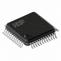
LPC1114FBD48/301,1 NXP Semiconductors, LPC1114FBD48/301,1 Datasheet - Page 23

LPC1114FBD48/301,1
Manufacturer Part Number
LPC1114FBD48/301,1
Description
IC MCU 32BIT 32KB FLASH 48LQFP
Manufacturer
NXP Semiconductors
Series
LPC1100r
Datasheets
1.LPC1114FHN333015.pdf
(2 pages)
2.LPC1114FHN333015.pdf
(66 pages)
3.LPC1114FHN333015.pdf
(66 pages)
Specifications of LPC1114FBD48/301,1
Program Memory Type
FLASH
Program Memory Size
32KB (32K x 8)
Package / Case
48-LQFP
Core Processor
ARM Cortex-M0
Core Size
32-Bit
Speed
50MHz
Connectivity
I²C, SPI, UART/USART
Peripherals
Brown-out Detect/Reset, POR, WDT
Number Of I /o
42
Ram Size
8K x 8
Voltage - Supply (vcc/vdd)
1.8 V ~ 3.6 V
Data Converters
A/D 8x10b
Oscillator Type
Internal
Operating Temperature
-40°C ~ 85°C
Processor Series
LPC11
Core
ARM Cortex M0
Data Bus Width
32 bit
Data Ram Size
8 KB
Interface Type
I2C, SPI, UART
Number Of Programmable I/os
28
Operating Supply Voltage
1.8 V to 3.6 V
Maximum Operating Temperature
+ 85 C
Mounting Style
SMD/SMT
3rd Party Development Tools
MDK-ARM, RL-ARM, ULINK2, KSK-LPC1114
Development Tools By Supplier
OM11049, OM11085
Minimum Operating Temperature
- 40 C
On-chip Adc
10 bit, 8 Channel
Lead Free Status / RoHS Status
Lead free / RoHS Compliant
For Use With
622-1005 - USB IN-CIRCUIT PROG ARM7 LPC2K
Eeprom Size
-
Lead Free Status / Rohs Status
Lead free / RoHS Compliant
Other names
568-4950
935290789151
935290789151
Available stocks
Company
Part Number
Manufacturer
Quantity
Price
Company:
Part Number:
LPC1114FBD48/301,1
Manufacturer:
SAMSUNG
Quantity:
1 085
Company:
Part Number:
LPC1114FBD48/301,1
Manufacturer:
NXP Semiconductors
Quantity:
10 000
NXP Semiconductors
LPC1111_12_13_14
Product data sheet
7.8.1 Features
7.9.1 Features
7.10 I
7.9 SPI serial I/O controller
Support for RS-485/9-bit mode allows both software address detection and automatic
address detection using 9-bit mode.
The UART includes a fractional baud rate generator. Standard baud rates such as
115200 Bd can be achieved with any crystal frequency above 2 MHz.
The LPC1111/12/13/14 contain two SPI controllers on the LQFP48/PLCC44 packages
and one SPI controller on the HVQFN33 packages (SPI0). Both SPI controllers support
SSP features.
The SPI controller is capable of operation on a SSP, 4-wire SSI, or Microwire bus. It can
interact with multiple masters and slaves on the bus. Only a single master and a single
slave can communicate on the bus during a given data transfer. The SPI supports full
duplex transfers, with frames of 4 bits to 16 bits of data flowing from the master to the
slave and from the slave to the master. In practice, often only one of these data flows
carries meaningful data.
The LPC1111/12/13/14 contain one I
The I
(SCL) and a Serial DAta line (SDA). Each device is recognized by a unique address and
can operate as either a receiver-only device (e.g., an LCD driver) or a transmitter with the
capability to both receive and send information (such as memory). Transmitters and/or
2
•
•
•
•
•
•
•
•
•
•
•
•
•
•
C-bus serial I/O controller
Maximum UART data bit rate of 3.125 MBit/s.
16 Byte Receive and Transmit FIFOs.
Register locations conform to 16C550 industry standard.
Receiver FIFO trigger points at 1 B, 4 B, 8 B, and 14 B.
Built-in fractional baud rate generator covering wide range of baud rates without a
need for external crystals of particular values.
FIFO control mechanism that enables software flow control implementation.
Support for RS-485/9-bit mode.
Support for modem control.
Maximum SPI speed of 25 Mbit/s (master) or 4.17 Mbit/s (slave) (in SSP mode)
Compatible with Motorola SPI, 4-wire Texas Instruments SSI, and National
Semiconductor Microwire buses
Synchronous serial communication
Master or slave operation
8-frame FIFOs for both transmit and receive
4-bit to 16-bit frame
2
C-bus is bidirectional for inter-IC control using only two wires: a Serial Clock Line
All information provided in this document is subject to legal disclaimers.
Rev. 4 — 10 February 2011
2
C-bus controller.
32-bit ARM Cortex-M0 microcontroller
LPC1111/12/13/14
© NXP B.V. 2011. All rights reserved.
23 of 66


