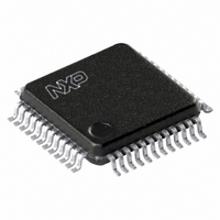
LPC1114FBD48/301,1 NXP Semiconductors, LPC1114FBD48/301,1 Datasheet - Page 51

LPC1114FBD48/301,1
Manufacturer Part Number
LPC1114FBD48/301,1
Description
IC MCU 32BIT 32KB FLASH 48LQFP
Manufacturer
NXP Semiconductors
Series
LPC1100r
Datasheets
1.LPC1114FHN333015.pdf
(2 pages)
2.LPC1114FHN333015.pdf
(66 pages)
3.LPC1114FHN333015.pdf
(66 pages)
Specifications of LPC1114FBD48/301,1
Program Memory Type
FLASH
Program Memory Size
32KB (32K x 8)
Package / Case
48-LQFP
Core Processor
ARM Cortex-M0
Core Size
32-Bit
Speed
50MHz
Connectivity
I²C, SPI, UART/USART
Peripherals
Brown-out Detect/Reset, POR, WDT
Number Of I /o
42
Ram Size
8K x 8
Voltage - Supply (vcc/vdd)
1.8 V ~ 3.6 V
Data Converters
A/D 8x10b
Oscillator Type
Internal
Operating Temperature
-40°C ~ 85°C
Processor Series
LPC11
Core
ARM Cortex M0
Data Bus Width
32 bit
Data Ram Size
8 KB
Interface Type
I2C, SPI, UART
Number Of Programmable I/os
28
Operating Supply Voltage
1.8 V to 3.6 V
Maximum Operating Temperature
+ 85 C
Mounting Style
SMD/SMT
3rd Party Development Tools
MDK-ARM, RL-ARM, ULINK2, KSK-LPC1114
Development Tools By Supplier
OM11049, OM11085
Minimum Operating Temperature
- 40 C
On-chip Adc
10 bit, 8 Channel
Lead Free Status / RoHS Status
Lead free / RoHS Compliant
For Use With
622-1005 - USB IN-CIRCUIT PROG ARM7 LPC2K
Eeprom Size
-
Lead Free Status / Rohs Status
Lead free / RoHS Compliant
Other names
568-4950
935290789151
935290789151
Available stocks
Company
Part Number
Manufacturer
Quantity
Price
Company:
Part Number:
LPC1114FBD48/301,1
Manufacturer:
SAMSUNG
Quantity:
1 085
Company:
Part Number:
LPC1114FBD48/301,1
Manufacturer:
NXP Semiconductors
Quantity:
10 000
NXP Semiconductors
LPC1111_12_13_14
Product data sheet
10.5 I/O pins
10.6 I
Table 16.
T
[1]
Table 17.
T
[1]
[2]
[3]
[4]
[5]
Symbol
t
t
Symbol
f
t
t
t
t
t
2
r
f
SCL
f
LOW
HIGH
HD;DAT
SU;DAT
amb
amb
C-bus
Applies to standard port pins and RESET pin.
See the I
Parameters are valid over operating temperature range unless otherwise specified.
t
and the acknowledge.
A device must internally provide a hold time of at least 300 ns for the SDA signal (with respect to the
V
C
HD;DAT
= −40 °C to +85 °C; 3.0 V ≤ V
= −40 °C to +85 °C.
IH
b
= total capacitance of one bus line in pF.
(min) of the SCL signal) to bridge the undefined region of the falling edge of SCL.
is the data hold time that is measured from the falling edge of SCL; applies to data in transmission
Dynamic characteristic: I/O pins
Dynamic characteristic: I
2
C-bus specification UM10204 for details.
Parameter
SCL clock
frequency
fall time
LOW period of
the SCL clock
HIGH period of
the SCL clock
data hold time
data set-up
time
All information provided in this document is subject to legal disclaimers.
Parameter
rise time
fall time
Rev. 4 — 10 February 2011
[2]
[4][5][6][7]
[3][4][8]
[9][10]
DD
Conditions
pin
configured as
output
pin
configured as
output
≤ 3.6 V.
2
C-bus pins
Conditions
Standard-mode
Fast-mode
Fast-mode Plus
of both SDA and
SCL signals
Standard-mode
Fast-mode
Fast-mode Plus
Standard-mode
Fast-mode
Fast-mode Plus
Standard-mode
Fast-mode
Fast-mode Plus
Standard-mode
Fast-mode
Fast-mode Plus
Standard-mode
Fast-mode
Fast-mode Plus
[1]
[1]
32-bit ARM Cortex-M0 microcontroller
Min
3.0
2.5
LPC1111/12/13/14
Min
0
0
0
-
20 + 0.1 × C
-
4.7
1.3
0.5
4.0
0.6
0.26
0
0
0
250
100
50
Typ
-
-
b
© NXP B.V. 2011. All rights reserved.
Max
100
400
1
300
300
120
-
-
-
-
-
-
-
-
-
-
-
-
Max
5.0
5.0
Unit
kHz
kHz
MHz
ns
ns
ns
μs
μs
μs
μs
μs
μs
μs
μs
μs
ns
ns
ns
Unit
ns
ns
51 of 66


