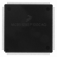
MC9S12XEP100CAG Freescale Semiconductor, MC9S12XEP100CAG Datasheet - Page 626

MC9S12XEP100CAG
Manufacturer Part Number
MC9S12XEP100CAG
Description
IC MCU 16BIT 1M FLASH 144-LQFP
Manufacturer
Freescale Semiconductor
Series
HCS12r
Datasheet
1.MC9S12XEP768CAL.pdf
(1328 pages)
Specifications of MC9S12XEP100CAG
Core Processor
HCS12X
Core Size
16-Bit
Speed
50MHz
Connectivity
CAN, EBI/EMI, I²C, IrDA, SCI, SPI
Peripherals
LVD, POR, PWM, WDT
Number Of I /o
119
Program Memory Size
1MB (1M x 8)
Program Memory Type
FLASH
Eeprom Size
4K x 8
Ram Size
64K x 8
Voltage - Supply (vcc/vdd)
1.72 V ~ 5.5 V
Data Converters
A/D 24x12b
Oscillator Type
External
Operating Temperature
-40°C ~ 85°C
Package / Case
144-LQFP
Processor Series
S12XE
Core
HCS12
Data Bus Width
16 bit
Data Ram Size
64 KB
Interface Type
CAN/SCI/SPI
Maximum Clock Frequency
50 MHz
Number Of Programmable I/os
119
Number Of Timers
25
Maximum Operating Temperature
+ 85 C
Mounting Style
SMD/SMT
3rd Party Development Tools
EWHCS12
Development Tools By Supplier
KIT33812ECUEVME, EVB9S12XEP100, DEMO9S12XEP100
Minimum Operating Temperature
- 40 C
On-chip Adc
24-ch x 12-bit
Cpu Family
HCS12X
Device Core Size
16b
Frequency (max)
50MHz
Total Internal Ram Size
64KB
# I/os (max)
119
Number Of Timers - General Purpose
25
Operating Supply Voltage (typ)
1.8/2.8/5V
Operating Supply Voltage (max)
1.98/2.9/5.5V
Operating Supply Voltage (min)
1.72/2.7/3.13V
Instruction Set Architecture
RISC
Operating Temp Range
-40C to 85C
Operating Temperature Classification
Industrial
Mounting
Surface Mount
Pin Count
144
Package Type
LQFP
Package
144LQFP
Family Name
HCS12X
Maximum Speed
50 MHz
Operating Supply Voltage
1.8|2.8|5 V
For Use With
EVB9S12XEP100 - BOARD EVAL FOR MC9S12XEP100DEMO9S12XEP100 - BOARD DEMO FOR MC9S12XEP100
Lead Free Status / RoHS Status
Lead free / RoHS Compliant
Available stocks
Company
Part Number
Manufacturer
Quantity
Price
Company:
Part Number:
MC9S12XEP100CAG
Manufacturer:
FREESCAL
Quantity:
244
Company:
Part Number:
MC9S12XEP100CAG
Manufacturer:
Freescale Semiconductor
Quantity:
10 000
- Current page: 626 of 1328
- Download datasheet (9Mb)
Chapter 16 Freescale’s Scalable Controller Area Network (S12MSCANV3)
The following gives a short programming example of the usage of the CANTBSEL register:
To get the next available transmit buffer, application software must read the CANTFLG register and write
this value back into the CANTBSEL register. In this example Tx buffers TX1 and TX2 are available. The
value read from CANTFLG is therefore 0b0000_0110. When writing this value back to CANTBSEL, the
Tx buffer TX1 is selected in the CANTXFG because the lowest numbered bit set to 1 is at bit position 1.
Reading back this value out of CANTBSEL results in 0b0000_0010, because only the lowest numbered
bit position set to 1 is presented. This mechanism eases the application software’s selection of the next
available Tx buffer.
If all transmit message buffers are deselected, no accesses are allowed to the CANTXFG registers.
16.3.2.12 MSCAN Identifier Acceptance Control Register (CANIDAC)
The CANIDAC register is used for identifier acceptance control as described below.
1. Read: Anytime
626
Module Base + 0x000B
Write: Anytime in initialization mode (INITRQ = 1 and INITAK = 1), except bits IDHITx, which are read-only
TX[2:0]
Field
•
•
•
2-0
Reset:
LDAA CANTFLG; value read is 0b0000_0110
STAA CANTBSEL; value written is 0b0000_0110
LDAA CANTBSEL; value read is 0b0000_0010
W
R
Transmit Buffer Select — The lowest numbered bit places the respective transmit buffer in the CANTXFG
register space (e.g., TX1 = 1 and TX0 = 1 selects transmit buffer TX0; TX1 = 1 and TX0 = 0 selects transmit
buffer TX1). Read and write accesses to the selected transmit buffer will be blocked, if the corresponding TXEx
bit is cleared and the buffer is scheduled for transmission (see
Register
0 The associated message buffer is deselected
1 The associated message buffer is selected, if lowest numbered bit
The CANTBSEL register is held in the reset state when the initialization
mode is active (INITRQ = 1 and INITAK=1). This register is writable when
not in initialization mode (INITRQ = 0 and INITAK = 0).
0
0
Figure 16-15. MSCAN Identifier Acceptance Control Register (CANIDAC)
7
(CANTFLG)”).
= Unimplemented
Table 16-17. CANTBSEL Register Field Descriptions
6
0
0
MC9S12XE-Family Reference Manual , Rev. 1.23
IDAM1
0
5
NOTE
IDAM0
4
0
Description
0
0
3
Section 16.3.2.7, “MSCAN Transmitter Flag
IDHIT2
2
0
Access: User read/write
Freescale Semiconductor
IDHIT1
0
1
IDHIT0
0
0
(1)
Related parts for MC9S12XEP100CAG
Image
Part Number
Description
Manufacturer
Datasheet
Request
R
Part Number:
Description:
Manufacturer:
Freescale Semiconductor, Inc
Datasheet:
Part Number:
Description:
Manufacturer:
Freescale Semiconductor, Inc
Datasheet:
Part Number:
Description:
Manufacturer:
Freescale Semiconductor, Inc
Datasheet:
Part Number:
Description:
Manufacturer:
Freescale Semiconductor, Inc
Datasheet:
Part Number:
Description:
Manufacturer:
Freescale Semiconductor, Inc
Datasheet:
Part Number:
Description:
Manufacturer:
Freescale Semiconductor, Inc
Datasheet:
Part Number:
Description:
Manufacturer:
Freescale Semiconductor, Inc
Datasheet:
Part Number:
Description:
Manufacturer:
Freescale Semiconductor, Inc
Datasheet:
Part Number:
Description:
Manufacturer:
Freescale Semiconductor, Inc
Datasheet:
Part Number:
Description:
Manufacturer:
Freescale Semiconductor, Inc
Datasheet:
Part Number:
Description:
Manufacturer:
Freescale Semiconductor, Inc
Datasheet:
Part Number:
Description:
Manufacturer:
Freescale Semiconductor, Inc
Datasheet:
Part Number:
Description:
Manufacturer:
Freescale Semiconductor, Inc
Datasheet:
Part Number:
Description:
Manufacturer:
Freescale Semiconductor, Inc
Datasheet:
Part Number:
Description:
Manufacturer:
Freescale Semiconductor, Inc
Datasheet:


