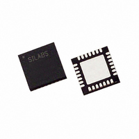
C8051F353-GM Silicon Laboratories Inc, C8051F353-GM Datasheet - Page 155

C8051F353-GM
Manufacturer Part Number
C8051F353-GM
Description
IC 8051 MCU 8K FLASH 28MLP
Manufacturer
Silicon Laboratories Inc
Series
C8051F35xr
Specifications of C8051F353-GM
Program Memory Type
FLASH
Program Memory Size
8KB (8K x 8)
Package / Case
28-VQFN Exposed Pad, 28-HVQFN, 28-SQFN, 28-DHVQFN
Core Processor
8051
Core Size
8-Bit
Speed
50MHz
Connectivity
SMBus (2-Wire/I²C), SPI, UART/USART
Peripherals
POR, PWM, Temp Sensor, WDT
Number Of I /o
17
Ram Size
768 x 8
Voltage - Supply (vcc/vdd)
2.7 V ~ 3.6 V
Data Converters
A/D 8x16b; D/A 2x8b
Oscillator Type
Internal
Operating Temperature
-40°C ~ 85°C
Processor Series
C8051F3x
Core
8051
Data Bus Width
8 bit
Data Ram Size
768 B
Interface Type
I2C/SMBus/SPI/UART
Maximum Clock Frequency
50 MHz
Number Of Programmable I/os
17
Number Of Timers
4
Operating Supply Voltage
2.7 V to 3.6 V
Maximum Operating Temperature
+ 85 C
Mounting Style
SMD/SMT
3rd Party Development Tools
KSK-SL-TOOLSTICK, PK51, CA51, A51, ULINK2
Development Tools By Supplier
C8051F350DK
Minimum Operating Temperature
- 40 C
On-chip Adc
8-ch x 16-bit
On-chip Dac
2-ch x 8-bit
No. Of I/o's
17
Ram Memory Size
768Byte
Cpu Speed
50MHz
No. Of Timers
4
Rohs Compliant
Yes
Package
28QFN
Device Core
8051
Family Name
C8051F35x
Maximum Speed
50 MHz
Data Rom Size
128 B
Height
0.88 mm
Length
5 mm
Supply Voltage (max)
3.6 V
Supply Voltage (min)
2.7 V
Width
5 mm
Lead Free Status / RoHS Status
Lead free / RoHS Compliant
For Use With
770-1006 - ISP 4PORT FOR SILABS C8051F MCU336-1083 - DEV KIT FOR F350/351/352/353
Eeprom Size
-
Lead Free Status / Rohs Status
Lead free / RoHS Compliant
Other names
336-1273
Available stocks
Company
Part Number
Manufacturer
Quantity
Price
Company:
Part Number:
C8051F353-GM
Manufacturer:
SiliconL
Quantity:
8 050
19.4. Using the SMBus
The SMBus can operate in both Master and Slave modes. The interface provides timing and shifting con-
trol for serial transfers; higher level protocol is determined by user software. The SMBus interface provides
the following application-independent features:
•
•
•
•
•
•
•
SMBus interrupts are generated for each data byte or slave address that is transferred. When transmitting,
this interrupt is generated after the ACK cycle so that software may read the received ACK value; when
receiving data, this interrupt is generated before the ACK cycle so that software may define the outgoing
ACK value. See Section “19.5. SMBus Transfer Modes’ on page 163 for more details on transmission
sequences.
Interrupts are also generated to indicate the beginning of a transfer when a master (START generated), or
the end of a transfer when a slave (STOP detected). Software should read the SMB0CN (SMBus Control
register) to find the cause of the SMBus interrupt. The SMB0CN register is described in Section
“19.4.2. SMB0CN Control Register’ on page 159; Table 19.4 provides a quick SMB0CN decoding refer-
ence.
SMBus configuration options include:
•
•
•
•
These options are selected in the SMB0CF register, as described in Section “19.4.1. SMBus Configuration
Register’ on page 156.
Byte-wise serial data transfers
Clock signal generation on SCL (Master Mode only) and SDA data synchronization
Timeout/bus error recognition, as defined by the SMB0CF configuration register
START/STOP timing, detection, and generation
Bus arbitration
Interrupt generation
Status information
Timeout detection (SCL Low Timeout and/or Bus Free Timeout)
SDA setup and hold time extensions
Slave event enable/disable
Clock source selection
Rev. 1.1
C8051F350/1/2/3
155


