C8051F353-GM Silicon Laboratories Inc, C8051F353-GM Datasheet - Page 88
C8051F353-GM
Manufacturer Part Number
C8051F353-GM
Description
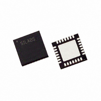
IC 8051 MCU 8K FLASH 28MLP
Manufacturer
Silicon Laboratories Inc
Series
C8051F35xr
Specifications of C8051F353-GM
Program Memory Type
FLASH
Program Memory Size
8KB (8K x 8)
Package / Case
28-VQFN Exposed Pad, 28-HVQFN, 28-SQFN, 28-DHVQFN
Core Processor
8051
Core Size
8-Bit
Speed
50MHz
Connectivity
SMBus (2-Wire/I²C), SPI, UART/USART
Peripherals
POR, PWM, Temp Sensor, WDT
Number Of I /o
17
Ram Size
768 x 8
Voltage - Supply (vcc/vdd)
2.7 V ~ 3.6 V
Data Converters
A/D 8x16b; D/A 2x8b
Oscillator Type
Internal
Operating Temperature
-40°C ~ 85°C
Processor Series
C8051F3x
Core
8051
Data Bus Width
8 bit
Data Ram Size
768 B
Interface Type
I2C/SMBus/SPI/UART
Maximum Clock Frequency
50 MHz
Number Of Programmable I/os
17
Number Of Timers
4
Operating Supply Voltage
2.7 V to 3.6 V
Maximum Operating Temperature
+ 85 C
Mounting Style
SMD/SMT
3rd Party Development Tools
KSK-SL-TOOLSTICK, PK51, CA51, A51, ULINK2
Development Tools By Supplier
C8051F350DK
Minimum Operating Temperature
- 40 C
On-chip Adc
8-ch x 16-bit
On-chip Dac
2-ch x 8-bit
No. Of I/o's
17
Ram Memory Size
768Byte
Cpu Speed
50MHz
No. Of Timers
4
Rohs Compliant
Yes
Package
28QFN
Device Core
8051
Family Name
C8051F35x
Maximum Speed
50 MHz
Data Rom Size
128 B
Height
0.88 mm
Length
5 mm
Supply Voltage (max)
3.6 V
Supply Voltage (min)
2.7 V
Width
5 mm
Lead Free Status / RoHS Status
Lead free / RoHS Compliant
For Use With
770-1006 - ISP 4PORT FOR SILABS C8051F MCU336-1083 - DEV KIT FOR F350/351/352/353
Eeprom Size
-
Lead Free Status / Rohs Status
Lead free / RoHS Compliant
Other names
336-1273
Available stocks
Company
Part Number
Manufacturer
Quantity
Price
Company:

Part Number:
C8051F353-GM
Manufacturer:
SiliconL
Quantity:
8 050


C8051F350/1/2/3
Performance
The CIP-51 employs a pipelined architecture that greatly increases its instruction throughput over the stan-
dard 8051 architecture. In a standard 8051, all instructions except for MUL and DIV take 12 or 24 system
clock cycles to execute, and usually have a maximum system clock of 12 MHz. By contrast, the CIP-51
core executes 70% of its instructions in one or two system clock cycles, with no instructions taking more
than eight system clock cycles.
With the CIP-51's system clock running at 50 MHz, it has a peak throughput of 50 MIPS. The CIP-51 has a
total of 109 instructions. The table below shows the total number of instructions that require each execution
time.
Programming and Debugging Support
In-system programming of the Flash program memory and communication with on-chip debug support
logic is accomplished via the Cygnal 2-Wire (C2) interface. Note that the re-programmable Flash can also
be read and changed a single byte at a time by the application software using the MOVC and MOVX
instructions. This feature allows program memory to be used for non-volatile data storage as well as updat-
ing program code under software control.
The on-chip debug support logic facilitates full speed in-circuit debugging, allowing the setting of hardware
breakpoints, starting, stopping and single stepping through program execution (including interrupt service
routines), examination of the program's call stack, and reading/writing the contents of registers and mem-
ory. This method of on-chip debugging is completely non-intrusive, requiring no RAM, Stack, timers, or
other on-chip resources.
The CIP-51 is supported by development tools from Silicon Labs and third party vendors. Silicon Labs pro-
vides an integrated development environment (IDE) including editor, macro assembler, debugger and pro-
grammer. The IDE's debugger and programmer interface to the CIP-51 via the on-chip debug logic to
provide fast and efficient in-system device programming and debugging. Third party macro assemblers
and C compilers are also available.
88
Number of Instructions
Clocks to Execute
26
1
50
2
2/3
Rev. 1.1
5
14
3
3/4
7
4
3
4/5
1
5
2
8
1
Related parts for C8051F353-GM
Image
Part Number
Description
Manufacturer
Datasheet
Request
R

Part Number:
Description:
SMD/C°/SINGLE-ENDED OUTPUT SILICON OSCILLATOR
Manufacturer:
Silicon Laboratories Inc
Part Number:
Description:
Manufacturer:
Silicon Laboratories Inc
Datasheet:
Part Number:
Description:
N/A N/A/SI4010 AES KEYFOB DEMO WITH LCD RX
Manufacturer:
Silicon Laboratories Inc
Datasheet:
Part Number:
Description:
N/A N/A/SI4010 SIMPLIFIED KEY FOB DEMO WITH LED RX
Manufacturer:
Silicon Laboratories Inc
Datasheet:
Part Number:
Description:
N/A/-40 TO 85 OC/EZLINK MODULE; F930/4432 HIGH BAND (REV E/B1)
Manufacturer:
Silicon Laboratories Inc
Part Number:
Description:
EZLink Module; F930/4432 Low Band (rev e/B1)
Manufacturer:
Silicon Laboratories Inc
Part Number:
Description:
I°/4460 10 DBM RADIO TEST CARD 434 MHZ
Manufacturer:
Silicon Laboratories Inc
Part Number:
Description:
I°/4461 14 DBM RADIO TEST CARD 868 MHZ
Manufacturer:
Silicon Laboratories Inc
Part Number:
Description:
I°/4463 20 DBM RFSWITCH RADIO TEST CARD 460 MHZ
Manufacturer:
Silicon Laboratories Inc
Part Number:
Description:
I°/4463 20 DBM RADIO TEST CARD 868 MHZ
Manufacturer:
Silicon Laboratories Inc
Part Number:
Description:
I°/4463 27 DBM RADIO TEST CARD 868 MHZ
Manufacturer:
Silicon Laboratories Inc
Part Number:
Description:
I°/4463 SKYWORKS 30 DBM RADIO TEST CARD 915 MHZ
Manufacturer:
Silicon Laboratories Inc
Part Number:
Description:
N/A N/A/-40 TO 85 OC/4463 RFMD 30 DBM RADIO TEST CARD 915 MHZ
Manufacturer:
Silicon Laboratories Inc
Part Number:
Description:
I°/4463 20 DBM RADIO TEST CARD 169 MHZ
Manufacturer:
Silicon Laboratories Inc