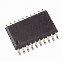
ATTINY461V-10SU Atmel, ATTINY461V-10SU Datasheet - Page 100

ATTINY461V-10SU
Manufacturer Part Number
ATTINY461V-10SU
Description
IC MCU AVR 4K FLASH 10MHZ 20SOIC
Manufacturer
Atmel
Series
AVR® ATtinyr
Specifications of ATTINY461V-10SU
Core Processor
AVR
Core Size
8-Bit
Speed
10MHz
Connectivity
USI
Peripherals
Brown-out Detect/Reset, POR, PWM, WDT
Number Of I /o
16
Program Memory Size
4KB (2K x 16)
Program Memory Type
FLASH
Eeprom Size
256 x 8
Ram Size
256 x 8
Voltage - Supply (vcc/vdd)
1.8 V ~ 5.5 V
Data Converters
A/D 11x10b
Oscillator Type
Internal
Operating Temperature
-40°C ~ 85°C
Package / Case
20-SOIC (7.5mm Width)
Processor Series
ATTINY4x
Core
AVR8
Data Bus Width
8 bit
Data Ram Size
256 B
Interface Type
2-Wire, SPI, USI
Maximum Clock Frequency
10 MHz
Number Of Programmable I/os
16
Number Of Timers
2
Operating Supply Voltage
2.7 V to 5.5 V
Maximum Operating Temperature
+ 85 C
Mounting Style
SMD/SMT
Minimum Operating Temperature
- 40 C
On-chip Adc
10 bit
Package
20SOIC W
Device Core
AVR
Family Name
ATtiny
Maximum Speed
10 MHz
For Use With
ATSTK600 - DEV KIT FOR AVR/AVR32ATAVRBC100 - REF DESIGN KIT BATTERY CHARGER770-1007 - ISP 4PORT ATMEL AVR MCU SPI/JTAG770-1004 - ISP 4PORT FOR ATMEL AVR MCU SPI
Lead Free Status / RoHS Status
Lead free / RoHS Compliant
Available stocks
Company
Part Number
Manufacturer
Quantity
Price
Part Number:
ATTINY461V-10SU
Manufacturer:
ATMEL/爱特梅尔
Quantity:
20 000
Part Number:
ATTINY461V-10SUR
Manufacturer:
ATMEL/爱特梅尔
Quantity:
20 000
12.8.2
100
ATtiny261/461/861
Fast PWM Mode
The counter value (TCNT1) that is shown as a histogram in
counter value matches the TOP value. The counter is then cleared at the following clock cycle
The diagram includes the Waveform Output (OCW1x) in toggle Compare Mode. The small hori-
zontal line marks on the TCNT1 slopes represent Compare Matches between OCR1x and
TCNT1.
The Timer/Counter Overflow Flag (TOV1) is set in the same clock cycle as the TCNT1 becomes
zero. The TOV1 Flag in this case behaves like a 11th bit, except that it is only set, not cleared.
However, combined with the timer overflow interrupt, that automatically clears the TOV1 Flag,
the timer resolution can be increased by software. There are no special cases to consider in the
Normal mode, a new counter value can be written anytime.
The Output Compare Unit can be used to generate interrupts at some given time. Using the Out-
put Compare to generate waveforms in Normal mode is not recommended, since this will
occupy too much of the CPU time. For generating a waveform, the OCW1x output can be set to
toggle its logical level on each Compare Match by setting the Compare Output mode bits to tog-
gle mode (COM1x1:0 = 1). The OC1x value will not be visible on the port pin unless the data
direction for the pin is set to output. The waveform generated will have a maximum frequency of
f
equation:
Resolution, R
and it can be calculated using the following equation:
The Output Compare Pin configurations in Normal Mode are described in
Table 12-2.
The fast Pulse Width Modulation or fast PWM mode (PWM1A/PWM1B = 1 and WGM11:10 = 00)
provides a high frequency PWM waveform generation option. The fast PWM differs from the
other PWM option by its single-slope operation. The counter counts from BOTTOM to TOP
(defined as OCR1C) then restarts from BOTTOM. In non-inverting Compare Output mode the
Waveform Output (OCW1x) is cleared on the Compare Match between TCNT1 and OCR1x and
set at BOTTOM. In inverting Compare Output mode, the Waveform Output is set on Compare
Match and cleared at BOTTOM. In complementary Compare Output mode the Waveform Output
is cleared on the Compare Match and set at BOTTOM.
Due to the single-slope operation, the operating frequency of the fast PWM mode can be twice
as high as the Phase and Frequency Correct PWM mode that use dual-slope operation. This
high frequency makes the fast PWM mode well suited for power regulation, rectification, and
OC1x
COM1x1
0
0
1
1
= f
clkT1
/4 when OCR1C is set to zero. The waveform frequency is defined by the following
PWM
Output Compare Pin Configurations in Normal Mode
, shows how many bit is required to express the value in the OCR1C register
COM1x0
0
1
0
1
f
OC1x
R
PWM
OC1x Pin
Disconnected
Disconnected
Disconnected
Disconnected
=
=
------------------------------------------ -
2
⋅
log
(
1
2
f
+
clkT1
(
OCR1C
OCR1C
)
+
1
Figure 12-11
)
OC1x Pin
Disconnected
OC1x
OC1x
OC1x
is incremented until the
Table
12-2.
2588E–AVR–08/10


