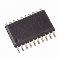
ATTINY461V-10SU Atmel, ATTINY461V-10SU Datasheet - Page 126

ATTINY461V-10SU
Manufacturer Part Number
ATTINY461V-10SU
Description
IC MCU AVR 4K FLASH 10MHZ 20SOIC
Manufacturer
Atmel
Series
AVR® ATtinyr
Specifications of ATTINY461V-10SU
Core Processor
AVR
Core Size
8-Bit
Speed
10MHz
Connectivity
USI
Peripherals
Brown-out Detect/Reset, POR, PWM, WDT
Number Of I /o
16
Program Memory Size
4KB (2K x 16)
Program Memory Type
FLASH
Eeprom Size
256 x 8
Ram Size
256 x 8
Voltage - Supply (vcc/vdd)
1.8 V ~ 5.5 V
Data Converters
A/D 11x10b
Oscillator Type
Internal
Operating Temperature
-40°C ~ 85°C
Package / Case
20-SOIC (7.5mm Width)
Processor Series
ATTINY4x
Core
AVR8
Data Bus Width
8 bit
Data Ram Size
256 B
Interface Type
2-Wire, SPI, USI
Maximum Clock Frequency
10 MHz
Number Of Programmable I/os
16
Number Of Timers
2
Operating Supply Voltage
2.7 V to 5.5 V
Maximum Operating Temperature
+ 85 C
Mounting Style
SMD/SMT
Minimum Operating Temperature
- 40 C
On-chip Adc
10 bit
Package
20SOIC W
Device Core
AVR
Family Name
ATtiny
Maximum Speed
10 MHz
For Use With
ATSTK600 - DEV KIT FOR AVR/AVR32ATAVRBC100 - REF DESIGN KIT BATTERY CHARGER770-1007 - ISP 4PORT ATMEL AVR MCU SPI/JTAG770-1004 - ISP 4PORT FOR ATMEL AVR MCU SPI
Lead Free Status / RoHS Status
Lead free / RoHS Compliant
Available stocks
Company
Part Number
Manufacturer
Quantity
Price
Part Number:
ATTINY461V-10SU
Manufacturer:
ATMEL/爱特梅尔
Quantity:
20 000
Part Number:
ATTINY461V-10SUR
Manufacturer:
ATMEL/爱特梅尔
Quantity:
20 000
- Current page: 126 of 242
- Download datasheet (5Mb)
13.3
13.3.1
126
Functional Descriptions
ATtiny261/461/861
Three-wire Mode
The 4-bit counter can be both read and written via the data bus, and it can generate an overflow
interrupt. The data register and the counter are clocked simultaneously by the same clock
source, allowing the counter to count the number of bits received or transmitted and generate an
interrupt when the transfer is complete. Note that when an external clock source is selected the
counter counts both clock edges. In this case the counter counts the number of edges, and not
the number of bits. The clock can be selected from three different sources: The USCK pin, the
Timer/Counter0 Compare Match or from software.
The Two-wire clock control unit can generate an interrupt when a start condition is detected on
the Two-wire bus. It can also generate wait states by holding the clock pin low after a start con-
dition is detected, or after the counter overflows.
The USI Three-wire mode is compliant to the Serial Peripheral Interface (SPI) mode 0 and 1, but
does not have the slave select (SS) pin functionality. However, this feature can be implemented
in software if necessary. Pin names used by this mode are: DI, DO, and USCK.
Figure 13-2. Three-wire Mode Operation, Simplified Diagram
Figure 13-2
The two USI Data Register are interconnected in such way that after eight USCK clocks, the
data in each register are interchanged. The same clock also increments the USI’s 4-bit counter.
The Counter Overflow (interrupt) Flag, or USIOIF, can therefore be used to determine when a
transfer is completed. The clock is generated by the Master device software by toggling the
USCK pin via the PORT Register or by writing a one to the USITC bit in USICR.
SLAVE
MASTER
Bit7
Bit7
shows two USI units operating in three-wire mode, one as Master and one as Slave.
Bit6
Bit6
Bit5
Bit5
Bit4
Bit4
Bit3
Bit3
Bit2
Bit2
Bit1
Bit1
Bit0
Bit0
PORTxn
USCK
USCK
DO
DO
DI
DI
2588E–AVR–08/10
Related parts for ATTINY461V-10SU
Image
Part Number
Description
Manufacturer
Datasheet
Request
R

Part Number:
Description:
Manufacturer:
Atmel Corporation
Datasheet:

Part Number:
Description:
Manufacturer:
Atmel Corporation
Datasheet:

Part Number:
Description:
IC AVR MCU 4K 20MHZ 32-QFN
Manufacturer:
Atmel
Datasheet:

Part Number:
Description:
IC MCU AVR 4K FLASH 20MHZ 20SOIC
Manufacturer:
Atmel
Datasheet:

Part Number:
Description:
MCU AVR 4K FLASH 15MHZ 32-QFN
Manufacturer:
Atmel
Datasheet:

Part Number:
Description:
MCU AVR 4KB FLASH 15MHZ 32-VQFN
Manufacturer:
Atmel
Datasheet:

Part Number:
Description:
MCU AVR 4KB FLASH 20MHZ 20SOIC
Manufacturer:
Atmel
Datasheet:

Part Number:
Description:
IC MCU AVR 4K 20MHZ 32QFN
Manufacturer:
Atmel
Datasheet:

Part Number:
Description:
Microcontrollers (MCU) 4kB Flash 0.256kB EEPROM 16 I/O Pins
Manufacturer:
Atmel
Datasheet:

Part Number:
Description:
IC, MCU, 8BIT, 2K FLASH, 20SOIC
Manufacturer:
Atmel
Datasheet:


