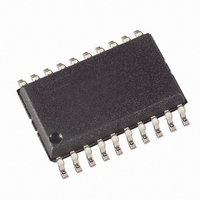
ATTINY461V-10SU Atmel, ATTINY461V-10SU Datasheet - Page 96

ATTINY461V-10SU
Manufacturer Part Number
ATTINY461V-10SU
Description
IC MCU AVR 4K FLASH 10MHZ 20SOIC
Manufacturer
Atmel
Series
AVR® ATtinyr
Specifications of ATTINY461V-10SU
Core Processor
AVR
Core Size
8-Bit
Speed
10MHz
Connectivity
USI
Peripherals
Brown-out Detect/Reset, POR, PWM, WDT
Number Of I /o
16
Program Memory Size
4KB (2K x 16)
Program Memory Type
FLASH
Eeprom Size
256 x 8
Ram Size
256 x 8
Voltage - Supply (vcc/vdd)
1.8 V ~ 5.5 V
Data Converters
A/D 11x10b
Oscillator Type
Internal
Operating Temperature
-40°C ~ 85°C
Package / Case
20-SOIC (7.5mm Width)
Processor Series
ATTINY4x
Core
AVR8
Data Bus Width
8 bit
Data Ram Size
256 B
Interface Type
2-Wire, SPI, USI
Maximum Clock Frequency
10 MHz
Number Of Programmable I/os
16
Number Of Timers
2
Operating Supply Voltage
2.7 V to 5.5 V
Maximum Operating Temperature
+ 85 C
Mounting Style
SMD/SMT
Minimum Operating Temperature
- 40 C
On-chip Adc
10 bit
Package
20SOIC W
Device Core
AVR
Family Name
ATtiny
Maximum Speed
10 MHz
For Use With
ATSTK600 - DEV KIT FOR AVR/AVR32ATAVRBC100 - REF DESIGN KIT BATTERY CHARGER770-1007 - ISP 4PORT ATMEL AVR MCU SPI/JTAG770-1004 - ISP 4PORT FOR ATMEL AVR MCU SPI
Lead Free Status / RoHS Status
Lead free / RoHS Compliant
Available stocks
Company
Part Number
Manufacturer
Quantity
Price
Part Number:
ATTINY461V-10SU
Manufacturer:
ATMEL/爱特梅尔
Quantity:
20 000
Part Number:
ATTINY461V-10SUR
Manufacturer:
ATMEL/爱特梅尔
Quantity:
20 000
- Current page: 96 of 242
- Download datasheet (5Mb)
12.6
96
Dead Time Generator
ATtiny261/461/861
The Dead Time Generator is provided for the Timer/Counter1 PWM output pairs to allow driving
external power control switches safely. The Dead Time Generator is a separate block that can
be used to insert dead times (non-overlapping times) for the Timer/Counter1 complementary
output pairs OC1x and OC1x when the PWM mode is enabled and the COM1x1:0 bits are set to
“01”. See
Figure 12-7. Block Diagram of Waveform Generator and Dead Time Generator.
The tasks are shared as follows: the Waveform Generator generates the output (OCW1x) and
the Dead Time Generator generates the non-overlapping PWM output pair from the output.
Three Dead Time Generators are provided, one for each PWM output. The non-overlap time is
adjustable and the PWM output and it’s complementary output are adjusted separately, and
independently for both PWM outputs.
The Dead Time Generation is based on 4-bit down counters that count the dead time, as shown
in
Figure 12-8. Dead Time Generator
There is a dedicated prescaler in front of the Dead Time Generator that can divide the
Timer/Counter1 clock (PCK or CK) by 1, 2, 4 or 8. This provides for large range of dead times
that can be generated. The prescaler is controlled by two control bits DTPS11:10. The block has
also a rising and falling edge detector that is used to start the dead time counting period.
Depending on the edge, one of the transitions on the rising edges, OC1x or OC1x is delayed
until the counter has counted to zero. The comparator is used to compare the counter with zero
and stop the dead time insertion when zero has been reached. The counter is loaded with a 4-bit
DT1H or DT1L value from DT1 I/O register, depending on the edge of the Waveform Output
(OCW1x) when the dead time insertion is started. The Output Compare Output are delayed by
one timer clock cycle at minimum from the Waveform Output when the Dead Time is adjusted to
CK OR PCK
bottom
OCWnx
FOCn
Figure
CLOCK
top
TCCRnB REGISTER
12-8.
Figure 12-7
PRE-SCALER
DEAD TIME
PWMnx
Waveform Generator
below.
WGM10
CLOCK CONTROL
COMnx
CK OR PCK
OCWnx
CLOCK
DTn I/O REGISTER
4-BIT COUNTER
COMPARATOR
DTPSn
Dead Time Generator
DATA BUS (8-bit)
DTnH
DTnL
OCnx
OCnx
PWM1X
PWM1X
2588E–AVR–08/10
OCnx
OCnx
OCnx
OCnx
pin
pin
Related parts for ATTINY461V-10SU
Image
Part Number
Description
Manufacturer
Datasheet
Request
R

Part Number:
Description:
Manufacturer:
Atmel Corporation
Datasheet:

Part Number:
Description:
Manufacturer:
Atmel Corporation
Datasheet:

Part Number:
Description:
IC AVR MCU 4K 20MHZ 32-QFN
Manufacturer:
Atmel
Datasheet:

Part Number:
Description:
IC MCU AVR 4K FLASH 20MHZ 20SOIC
Manufacturer:
Atmel
Datasheet:

Part Number:
Description:
MCU AVR 4K FLASH 15MHZ 32-QFN
Manufacturer:
Atmel
Datasheet:

Part Number:
Description:
MCU AVR 4KB FLASH 15MHZ 32-VQFN
Manufacturer:
Atmel
Datasheet:

Part Number:
Description:
MCU AVR 4KB FLASH 20MHZ 20SOIC
Manufacturer:
Atmel
Datasheet:

Part Number:
Description:
IC MCU AVR 4K 20MHZ 32QFN
Manufacturer:
Atmel
Datasheet:

Part Number:
Description:
Microcontrollers (MCU) 4kB Flash 0.256kB EEPROM 16 I/O Pins
Manufacturer:
Atmel
Datasheet:

Part Number:
Description:
IC, MCU, 8BIT, 2K FLASH, 20SOIC
Manufacturer:
Atmel
Datasheet:


