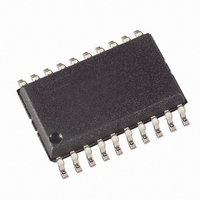
ATTINY461V-10SU Atmel, ATTINY461V-10SU Datasheet - Page 177

ATTINY461V-10SU
Manufacturer Part Number
ATTINY461V-10SU
Description
IC MCU AVR 4K FLASH 10MHZ 20SOIC
Manufacturer
Atmel
Series
AVR® ATtinyr
Specifications of ATTINY461V-10SU
Core Processor
AVR
Core Size
8-Bit
Speed
10MHz
Connectivity
USI
Peripherals
Brown-out Detect/Reset, POR, PWM, WDT
Number Of I /o
16
Program Memory Size
4KB (2K x 16)
Program Memory Type
FLASH
Eeprom Size
256 x 8
Ram Size
256 x 8
Voltage - Supply (vcc/vdd)
1.8 V ~ 5.5 V
Data Converters
A/D 11x10b
Oscillator Type
Internal
Operating Temperature
-40°C ~ 85°C
Package / Case
20-SOIC (7.5mm Width)
Processor Series
ATTINY4x
Core
AVR8
Data Bus Width
8 bit
Data Ram Size
256 B
Interface Type
2-Wire, SPI, USI
Maximum Clock Frequency
10 MHz
Number Of Programmable I/os
16
Number Of Timers
2
Operating Supply Voltage
2.7 V to 5.5 V
Maximum Operating Temperature
+ 85 C
Mounting Style
SMD/SMT
Minimum Operating Temperature
- 40 C
On-chip Adc
10 bit
Package
20SOIC W
Device Core
AVR
Family Name
ATtiny
Maximum Speed
10 MHz
For Use With
ATSTK600 - DEV KIT FOR AVR/AVR32ATAVRBC100 - REF DESIGN KIT BATTERY CHARGER770-1007 - ISP 4PORT ATMEL AVR MCU SPI/JTAG770-1004 - ISP 4PORT FOR ATMEL AVR MCU SPI
Lead Free Status / RoHS Status
Lead free / RoHS Compliant
Available stocks
Company
Part Number
Manufacturer
Quantity
Price
Part Number:
ATTINY461V-10SU
Manufacturer:
ATMEL/爱特梅尔
Quantity:
20 000
Part Number:
ATTINY461V-10SUR
Manufacturer:
ATMEL/爱特梅尔
Quantity:
20 000
- Current page: 177 of 242
- Download datasheet (5Mb)
Figure 18-2. Serial Programming Instruction example
18.7
18.7.1
2588E–AVR–08/10
Byte 1
Parallel Programming
Signal Names
Load Program Memory Page (High/Low Byte)/
Load EEPROM Memory Page (page access)
Bit 15 B
Byte 2
Adr MSB
Adr dr M
A
r MS S B
If the LSB in RDY/BSY data byte out is ‘1’, a programming operation is still pending. Wait until
this bit returns ‘0’ before the next instruction is carried out.
Within the same page, the low data byte must be loaded prior to the high data byte.
After data is loaded to the page buffer, program the EEPROM page, see
177.
This section describes how to parallel program and verify Flash Program memory, EEPROM
Data memory, Memory Lock bits, and Fuse bits. Pulses are assumed to be at least 250 ns in
length, unless otherwise noted.
In this section, some pins are referenced by signal names describing their functionality during
parallel programming, see
are referenced by pin names.
Byte 3
Adr LSB
Page Offset
0
Serial Programming Instruction
Byte 4
Program Memory/
EEPROM Memory
Figure 18-3
Page Buffer
Page N-1
Page 0
Page 1
Page 2
and
Byte 1
Table
Page Number
18-12. Pins not described in the following table
Bit 15 B
Byte 2
Write Program Memory Page/
Write EEPROM Memory Page
Adr MSB
Byte 3
Adr LSB
A A dr dr LS
LSB
SB
Figure 18-2 on page
0
Byte 4
177
Related parts for ATTINY461V-10SU
Image
Part Number
Description
Manufacturer
Datasheet
Request
R

Part Number:
Description:
Manufacturer:
Atmel Corporation
Datasheet:

Part Number:
Description:
Manufacturer:
Atmel Corporation
Datasheet:

Part Number:
Description:
IC AVR MCU 4K 20MHZ 32-QFN
Manufacturer:
Atmel
Datasheet:

Part Number:
Description:
IC MCU AVR 4K FLASH 20MHZ 20SOIC
Manufacturer:
Atmel
Datasheet:

Part Number:
Description:
MCU AVR 4K FLASH 15MHZ 32-QFN
Manufacturer:
Atmel
Datasheet:

Part Number:
Description:
MCU AVR 4KB FLASH 15MHZ 32-VQFN
Manufacturer:
Atmel
Datasheet:

Part Number:
Description:
MCU AVR 4KB FLASH 20MHZ 20SOIC
Manufacturer:
Atmel
Datasheet:

Part Number:
Description:
IC MCU AVR 4K 20MHZ 32QFN
Manufacturer:
Atmel
Datasheet:

Part Number:
Description:
Microcontrollers (MCU) 4kB Flash 0.256kB EEPROM 16 I/O Pins
Manufacturer:
Atmel
Datasheet:

Part Number:
Description:
IC, MCU, 8BIT, 2K FLASH, 20SOIC
Manufacturer:
Atmel
Datasheet:


