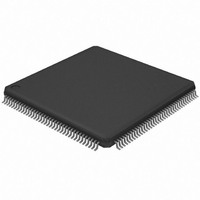
AT32UC3A0512-ALTTA Atmel, AT32UC3A0512-ALTTA Datasheet - Page 270

AT32UC3A0512-ALTTA
Manufacturer Part Number
AT32UC3A0512-ALTTA
Description
IC MCU AVR32 512K FLASH 144LQFP
Manufacturer
Atmel
Series
AVR®32 UC3r
Datasheet
1.ATEVK1104.pdf
(826 pages)
Specifications of AT32UC3A0512-ALTTA
Core Processor
AVR
Core Size
32-Bit
Speed
66MHz
Connectivity
EBI/EMI, Ethernet, I²C, SPI, SSC, UART/USART, USB OTG
Peripherals
Brown-out Detect/Reset, POR, PWM, WDT
Number Of I /o
109
Program Memory Size
512KB (512K x 8)
Program Memory Type
FLASH
Ram Size
64K x 8
Voltage - Supply (vcc/vdd)
1.65 V ~ 1.95 V
Data Converters
A/D 8x10b
Oscillator Type
Internal
Operating Temperature
-40°C ~ 85°C
Package / Case
144-LQFP
Lead Free Status / RoHS Status
Lead free / RoHS Compliant
Eeprom Size
-
Available stocks
Company
Part Number
Manufacturer
Quantity
Price
- Current page: 270 of 826
- Download datasheet (20Mb)
25.7.6
25.7.6.1
25.7.7
32058J-AVR32-04/11
Receive Compare Modes
Data Format
Compare Functions
Figure 25-12. Receive Compare Modes
Compare 0 can be one start event of the Receiver. In this case, the receiver compares at each
new sample the last FSLEN bits received at the FSLEN lower bit of the data contained in the
Compare 0 Register (RC0R). When this start event is selected, the user can program the
Receiver to start a new data transfer either by writing a new Compare 0, or by receiving continu-
ously until Compare 1 occurs. This selection is done with the bit (STOP) in RCMR.
The data framing format of both the transmitter and the receiver are programmable through the
Transmitter Frame Mode Register (TFMR) and the Receiver Frame Mode Register (RFMR). In
either case, the user can independently select:
Additionally, the transmitter can be used to transfer synchronization and select the level driven
on the TX_DATA pin while not in data transfer operation. This is done respectively by the Frame
Sync Data Enable (FSDEN) and by the Data Default Value (DATDEF) bits in TFMR.
• the event that starts the data transfer (START)
• the delay in number of bit periods between the start event and the first data bit (
• the length of the data (DATLEN)
• the number of data to be transferred for each start event (DATNB).
• the length of synchronization transferred for each start event (FSLEN)
• the bit sense: most or lowest significant bit first (MSBF).
RX_CLOCK
RX_DATA
(Input)
CMP0
(4 in This Example)
CMP1
Up to 16 Bits
FSLEN
CMP2
CMP3
Start
STTDLY
Ignored
B0
DATLEN
AT32UC3A
B1
B2
STTDLY
)
270
Related parts for AT32UC3A0512-ALTTA
Image
Part Number
Description
Manufacturer
Datasheet
Request
R

Part Number:
Description:
MCU, MPU & DSP Development Tools KICKSTART KIT FOR AT32UC3A
Manufacturer:
IAR Systems

Part Number:
Description:
DEV KIT FOR AVR/AVR32
Manufacturer:
Atmel
Datasheet:

Part Number:
Description:
INTERVAL AND WIPE/WASH WIPER CONTROL IC WITH DELAY
Manufacturer:
ATMEL Corporation
Datasheet:

Part Number:
Description:
Low-Voltage Voice-Switched IC for Hands-Free Operation
Manufacturer:
ATMEL Corporation
Datasheet:

Part Number:
Description:
MONOLITHIC INTEGRATED FEATUREPHONE CIRCUIT
Manufacturer:
ATMEL Corporation
Datasheet:

Part Number:
Description:
AM-FM Receiver IC U4255BM-M
Manufacturer:
ATMEL Corporation
Datasheet:

Part Number:
Description:
Monolithic Integrated Feature Phone Circuit
Manufacturer:
ATMEL Corporation
Datasheet:

Part Number:
Description:
Multistandard Video-IF and Quasi Parallel Sound Processing
Manufacturer:
ATMEL Corporation
Datasheet:

Part Number:
Description:
High-performance EE PLD
Manufacturer:
ATMEL Corporation
Datasheet:

Part Number:
Description:
8-bit Flash Microcontroller
Manufacturer:
ATMEL Corporation
Datasheet:

Part Number:
Description:
2-Wire Serial EEPROM
Manufacturer:
ATMEL Corporation
Datasheet:


