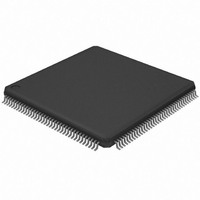
AT32UC3A0512-ALTTA Atmel, AT32UC3A0512-ALTTA Datasheet - Page 382

AT32UC3A0512-ALTTA
Manufacturer Part Number
AT32UC3A0512-ALTTA
Description
IC MCU AVR32 512K FLASH 144LQFP
Manufacturer
Atmel
Series
AVR®32 UC3r
Datasheet
1.ATEVK1104.pdf
(826 pages)
Specifications of AT32UC3A0512-ALTTA
Core Processor
AVR
Core Size
32-Bit
Speed
66MHz
Connectivity
EBI/EMI, Ethernet, I²C, SPI, SSC, UART/USART, USB OTG
Peripherals
Brown-out Detect/Reset, POR, PWM, WDT
Number Of I /o
109
Program Memory Size
512KB (512K x 8)
Program Memory Type
FLASH
Ram Size
64K x 8
Voltage - Supply (vcc/vdd)
1.65 V ~ 1.95 V
Data Converters
A/D 8x10b
Oscillator Type
Internal
Operating Temperature
-40°C ~ 85°C
Package / Case
144-LQFP
Lead Free Status / RoHS Status
Lead free / RoHS Compliant
Eeprom Size
-
Available stocks
Company
Part Number
Manufacturer
Quantity
Price
- Current page: 382 of 826
- Download datasheet (20Mb)
Table 27-3.
27.6.4.7
27.6.5
32058J–AVR32–04/11
Coded Value
setup [5:0]
pulse [6:0]
cycle [8:0]
Automatic Wait States
Usage Restriction
Coding and Range of Timing Parameters
Number of Bits
The SETUP register groups the definition of all setup parameters:
• NRD_SETUP, NCS_RD_SETUP, NWE_SETUP, NCS_WR_SETUP
The PULSE register groups the definition of all pulse parameters:
• NRD_PULSE, ncs_rd_pULSE, nwe_pULSE, ncs_wr_pULSE
The CYCLE register groups the definition of all cycle parameters:
• NRD_CYCLE, NWE_CYCLEe
Table 27-3
The SMC does not check the validity of the user-programmed parameters. If the sum of
SETUP and PULSE parameters is larger than the corresponding CYCLE parameter, this
leads to unpredictable behavior of the SMC.
For read operations:
Null but positive setup and hold of address and NRD and/or NCS can not be guaranteed at the
memory interface because of the propagation delay of theses signals through external logic and
pads. If positive setup and hold values must be verified, then it is strictly recommended to pro-
gram non-null values so as to cover possible skews between address, NCS and NRD signals.
For write operations:
If a null hold value is programmed on NWE, the SMC can guarantee a positive hold of address,
byte select lines, and NCS signal after the rising edge of NWE. This is true for WRITE_MODE =
1 only. See
For read and write operations: a null value for pulse parameters is forbidden and may lead to
unpredictable behavior.
In read and write cycles, the setup and hold time parameters are defined in reference to the
address bus. For external devices that require setup and hold time between NCS and NRD sig-
nals (read), or between NCS and NWE signals (write), these setup and hold times must be
converted into setup and hold times in reference to the address bus.
Under certain circumstances, the SMC automatically inserts idle cycles between accesses to
avoid bus contention or operation conflict.
6
7
9
shows how the timing parameters are coded and their permitted range.
”Early Read Wait State” on page
256 x cycle[8:7] + cycle[6:0]
128 x setup[5] + setup[4:0]
256 x pulse[6] + pulse[5:0]
Effective Value
385.
Coded Value
0 ≤ ≤ 127
0 ≤ ≤ 31
0 ≤ ≤ 63
Permitted Range
AT32UC3A
256 ≤ ≤ 256+127
512 ≤ ≤ 512+127
768 ≤ ≤ 768+127
Effective Value
128 ≤ ≤ 128+31
256 ≤ ≤ 256+63
382
Related parts for AT32UC3A0512-ALTTA
Image
Part Number
Description
Manufacturer
Datasheet
Request
R

Part Number:
Description:
MCU, MPU & DSP Development Tools KICKSTART KIT FOR AT32UC3A
Manufacturer:
IAR Systems

Part Number:
Description:
DEV KIT FOR AVR/AVR32
Manufacturer:
Atmel
Datasheet:

Part Number:
Description:
INTERVAL AND WIPE/WASH WIPER CONTROL IC WITH DELAY
Manufacturer:
ATMEL Corporation
Datasheet:

Part Number:
Description:
Low-Voltage Voice-Switched IC for Hands-Free Operation
Manufacturer:
ATMEL Corporation
Datasheet:

Part Number:
Description:
MONOLITHIC INTEGRATED FEATUREPHONE CIRCUIT
Manufacturer:
ATMEL Corporation
Datasheet:

Part Number:
Description:
AM-FM Receiver IC U4255BM-M
Manufacturer:
ATMEL Corporation
Datasheet:

Part Number:
Description:
Monolithic Integrated Feature Phone Circuit
Manufacturer:
ATMEL Corporation
Datasheet:

Part Number:
Description:
Multistandard Video-IF and Quasi Parallel Sound Processing
Manufacturer:
ATMEL Corporation
Datasheet:

Part Number:
Description:
High-performance EE PLD
Manufacturer:
ATMEL Corporation
Datasheet:

Part Number:
Description:
8-bit Flash Microcontroller
Manufacturer:
ATMEL Corporation
Datasheet:

Part Number:
Description:
2-Wire Serial EEPROM
Manufacturer:
ATMEL Corporation
Datasheet:


