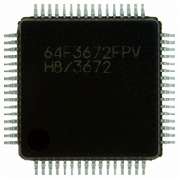
HD64F3672FPV Renesas Electronics America, HD64F3672FPV Datasheet - Page 172

HD64F3672FPV
Manufacturer Part Number
HD64F3672FPV
Description
IC H8/3672 MCU FLASH 64LQFP
Manufacturer
Renesas Electronics America
Series
H8® H8/300H Tinyr
Datasheets
1.DF36912GFHV.pdf
(277 pages)
2.DF36012GFYV.pdf
(1021 pages)
3.HD64F3672FXV.pdf
(334 pages)
Specifications of HD64F3672FPV
Core Processor
H8/300H
Core Size
16-Bit
Speed
16MHz
Connectivity
SCI
Peripherals
PWM, WDT
Number Of I /o
26
Program Memory Size
16KB (16K x 8)
Program Memory Type
FLASH
Ram Size
2K x 8
Voltage - Supply (vcc/vdd)
3 V ~ 5.5 V
Data Converters
A/D 4x10b
Oscillator Type
Internal
Operating Temperature
-20°C ~ 75°C
Package / Case
64-LQFP
For Use With
R0K436079S000BE - KIT DEV FOR H8/36079 W/COMPILER
Lead Free Status / RoHS Status
Lead free / RoHS Compliant
Eeprom Size
-
Available stocks
Company
Part Number
Manufacturer
Quantity
Price
Company:
Part Number:
HD64F3672FPV
Manufacturer:
MICROCHIP
Quantity:
1 000
Company:
Part Number:
HD64F3672FPV
Manufacturer:
Renesas Electronics America
Quantity:
135
Company:
Part Number:
HD64F3672FPV
Manufacturer:
Renesas Electronics America
Quantity:
10 000
Part Number:
HD64F3672FPV
Manufacturer:
RENESAS/瑞萨
Quantity:
20 000
- Current page: 172 of 334
- Download datasheet (2Mb)
Section 11 Timer W
11.4.2
In PWM mode, PWM waveforms are generated by using GRA as the period register and GRB,
GRC, and GRD as duty registers. PWM waveforms are output from the FTIOB, FTIOC, and
FTIOD pins. Up to three-phase PWM waveforms can be output. In PWM mode, a general register
functions as an output compare register automatically. The output level of each pin depends on the
corresponding timer output level set bit (TOB, TOC, and TOD) in TCRW. When TOB is 1, the
FTIOB output goes to 1 at compare match A and to 0 at compare match B. When TOB is 0, the
FTIOB output goes to 0 at compare match A and to 1 at compare match B. Thus the compare
match output level settings in TIOR0 and TIOR1 are ignored for the output pin set to PWM mode.
If the same value is set in the cycle register and the duty register, the output does not change when
a compare match occurs.
Figure 11.9 shows an example of operation in PWM mode. The output signals go to 1 and TCNT
is cleared at compare match A, and the output signals go to 0 at compare match B, C, and D (TOB,
TOC, and TOD = 1: initial output values are set to 1).
Rev.4.00 Nov. 02, 2005 Page 146 of 304
REJ09B0143-0400
PWM Operation
H'FFFF
H'DA91
H'5480
H'0245
H'0000
FTIOA
GRA
GRC
Figure 11.8 Buffer Operation Example (Input Capture)
TCNT value
H'0245
H'5480
H'0245
H'DA91
H'5480
Time
Related parts for HD64F3672FPV
Image
Part Number
Description
Manufacturer
Datasheet
Request
R

Part Number:
Description:
KIT STARTER FOR M16C/29
Manufacturer:
Renesas Electronics America
Datasheet:

Part Number:
Description:
KIT STARTER FOR R8C/2D
Manufacturer:
Renesas Electronics America
Datasheet:

Part Number:
Description:
R0K33062P STARTER KIT
Manufacturer:
Renesas Electronics America
Datasheet:

Part Number:
Description:
KIT STARTER FOR R8C/23 E8A
Manufacturer:
Renesas Electronics America
Datasheet:

Part Number:
Description:
KIT STARTER FOR R8C/25
Manufacturer:
Renesas Electronics America
Datasheet:

Part Number:
Description:
KIT STARTER H8S2456 SHARPE DSPLY
Manufacturer:
Renesas Electronics America
Datasheet:

Part Number:
Description:
KIT STARTER FOR R8C38C
Manufacturer:
Renesas Electronics America
Datasheet:

Part Number:
Description:
KIT STARTER FOR R8C35C
Manufacturer:
Renesas Electronics America
Datasheet:

Part Number:
Description:
KIT STARTER FOR R8CL3AC+LCD APPS
Manufacturer:
Renesas Electronics America
Datasheet:

Part Number:
Description:
KIT STARTER FOR RX610
Manufacturer:
Renesas Electronics America
Datasheet:

Part Number:
Description:
KIT STARTER FOR R32C/118
Manufacturer:
Renesas Electronics America
Datasheet:

Part Number:
Description:
KIT DEV RSK-R8C/26-29
Manufacturer:
Renesas Electronics America
Datasheet:

Part Number:
Description:
KIT STARTER FOR SH7124
Manufacturer:
Renesas Electronics America
Datasheet:

Part Number:
Description:
KIT STARTER FOR H8SX/1622
Manufacturer:
Renesas Electronics America
Datasheet:


