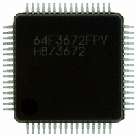
HD64F3672FPV Renesas Electronics America, HD64F3672FPV Datasheet - Page 184

HD64F3672FPV
Manufacturer Part Number
HD64F3672FPV
Description
IC H8/3672 MCU FLASH 64LQFP
Manufacturer
Renesas Electronics America
Series
H8® H8/300H Tinyr
Datasheets
1.DF36912GFHV.pdf
(277 pages)
2.DF36012GFYV.pdf
(1021 pages)
3.HD64F3672FXV.pdf
(334 pages)
Specifications of HD64F3672FPV
Core Processor
H8/300H
Core Size
16-Bit
Speed
16MHz
Connectivity
SCI
Peripherals
PWM, WDT
Number Of I /o
26
Program Memory Size
16KB (16K x 8)
Program Memory Type
FLASH
Ram Size
2K x 8
Voltage - Supply (vcc/vdd)
3 V ~ 5.5 V
Data Converters
A/D 4x10b
Oscillator Type
Internal
Operating Temperature
-20°C ~ 75°C
Package / Case
64-LQFP
For Use With
R0K436079S000BE - KIT DEV FOR H8/36079 W/COMPILER
Lead Free Status / RoHS Status
Lead free / RoHS Compliant
Eeprom Size
-
Available stocks
Company
Part Number
Manufacturer
Quantity
Price
Company:
Part Number:
HD64F3672FPV
Manufacturer:
MICROCHIP
Quantity:
1 000
Company:
Part Number:
HD64F3672FPV
Manufacturer:
Renesas Electronics America
Quantity:
135
Company:
Part Number:
HD64F3672FPV
Manufacturer:
Renesas Electronics America
Quantity:
10 000
Part Number:
HD64F3672FPV
Manufacturer:
RENESAS/瑞萨
Quantity:
20 000
- Current page: 184 of 334
- Download datasheet (2Mb)
Section 11 Timer W
5. The TOA to TOD bits in TCRW decide the value of the FTIO pin, which is output until the
Compare match
signal B
Rev.4.00 Nov. 02, 2005 Page 158 of 304
REJ09B0143-0400
BCLR#2, @TCRW
(1) TCRW read operation: Read H'06
(2) Modify operation: Modify H'06 to H'02
(3) Write operation to TCRW: Write H'02
TCRW has been set to H'06. Compare match B and compare match C are used. The FTIOB pin is in the 1 output state,
and is set to the toggle output or the 0 output by compare match B.
When BCLR#2, @TCRW is executed to clear the TOC bit (the FTIOC signal is low) and compare match B occurs
at the same timing as shown below, the H'02 writing to TCRW has priority and compare match B does not drive the FTIOB signal low;
the FTIOB signal remains high.
first compare match occurs. Once a compare match occurs and this compare match changes the
values of FTIOA to FTIOD output, the values of the FTIOA to FTIOD pin output and the
values read from the TOA to TOD bits may differ. Moreover, when the writing to TCRW and
the generation of the compare match A to D occur at the same timing, the writing to TCRW
has the priority. Thus, output change due to the compare match is not reflected to the FTIOA
to FTIOD pins. Therefore, when bit manipulation instruction is used to write to TCRW, the
values of the FTIOA to FTIOD pin output may result in an unexpected result. When TCRW is
to be written to while compare match is operating, stop the counter once before accessing to
TCRW, read the port 8 state to reflect the values of FTIOA to FTIOD output, to TOA to TOD,
and then restart the counter. Figure 11.26 shows an example when the compare match and the
bit manipulation instruction to TCRW occur at the same timing.
Bit
TCRW
Set value
TCRW
write signal
FTIOB pin
Figure 11.26 When Compare Match and Bit Manipulation Instruction to TCRW
φ
CCLR
7
0
CKS2
6
0
CKS1
5
0
Occur at the Same Timing
CKS0
4
0
TOD
Remains high because the 1 writing to TOB has priority
3
0
TOC
2
1
TOB
1
1
TOA
0
0
Expected output
Related parts for HD64F3672FPV
Image
Part Number
Description
Manufacturer
Datasheet
Request
R

Part Number:
Description:
KIT STARTER FOR M16C/29
Manufacturer:
Renesas Electronics America
Datasheet:

Part Number:
Description:
KIT STARTER FOR R8C/2D
Manufacturer:
Renesas Electronics America
Datasheet:

Part Number:
Description:
R0K33062P STARTER KIT
Manufacturer:
Renesas Electronics America
Datasheet:

Part Number:
Description:
KIT STARTER FOR R8C/23 E8A
Manufacturer:
Renesas Electronics America
Datasheet:

Part Number:
Description:
KIT STARTER FOR R8C/25
Manufacturer:
Renesas Electronics America
Datasheet:

Part Number:
Description:
KIT STARTER H8S2456 SHARPE DSPLY
Manufacturer:
Renesas Electronics America
Datasheet:

Part Number:
Description:
KIT STARTER FOR R8C38C
Manufacturer:
Renesas Electronics America
Datasheet:

Part Number:
Description:
KIT STARTER FOR R8C35C
Manufacturer:
Renesas Electronics America
Datasheet:

Part Number:
Description:
KIT STARTER FOR R8CL3AC+LCD APPS
Manufacturer:
Renesas Electronics America
Datasheet:

Part Number:
Description:
KIT STARTER FOR RX610
Manufacturer:
Renesas Electronics America
Datasheet:

Part Number:
Description:
KIT STARTER FOR R32C/118
Manufacturer:
Renesas Electronics America
Datasheet:

Part Number:
Description:
KIT DEV RSK-R8C/26-29
Manufacturer:
Renesas Electronics America
Datasheet:

Part Number:
Description:
KIT STARTER FOR SH7124
Manufacturer:
Renesas Electronics America
Datasheet:

Part Number:
Description:
KIT STARTER FOR H8SX/1622
Manufacturer:
Renesas Electronics America
Datasheet:


