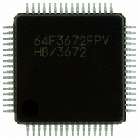
HD64F3672FPV Renesas Electronics America, HD64F3672FPV Datasheet - Page 189

HD64F3672FPV
Manufacturer Part Number
HD64F3672FPV
Description
IC H8/3672 MCU FLASH 64LQFP
Manufacturer
Renesas Electronics America
Series
H8® H8/300H Tinyr
Datasheets
1.DF36912GFHV.pdf
(277 pages)
2.DF36012GFYV.pdf
(1021 pages)
3.HD64F3672FXV.pdf
(334 pages)
Specifications of HD64F3672FPV
Core Processor
H8/300H
Core Size
16-Bit
Speed
16MHz
Connectivity
SCI
Peripherals
PWM, WDT
Number Of I /o
26
Program Memory Size
16KB (16K x 8)
Program Memory Type
FLASH
Ram Size
2K x 8
Voltage - Supply (vcc/vdd)
3 V ~ 5.5 V
Data Converters
A/D 4x10b
Oscillator Type
Internal
Operating Temperature
-20°C ~ 75°C
Package / Case
64-LQFP
For Use With
R0K436079S000BE - KIT DEV FOR H8/36079 W/COMPILER
Lead Free Status / RoHS Status
Lead free / RoHS Compliant
Eeprom Size
-
Available stocks
Company
Part Number
Manufacturer
Quantity
Price
Company:
Part Number:
HD64F3672FPV
Manufacturer:
MICROCHIP
Quantity:
1 000
Company:
Part Number:
HD64F3672FPV
Manufacturer:
Renesas Electronics America
Quantity:
135
Company:
Part Number:
HD64F3672FPV
Manufacturer:
Renesas Electronics America
Quantity:
10 000
Part Number:
HD64F3672FPV
Manufacturer:
RENESAS/瑞萨
Quantity:
20 000
- Current page: 189 of 334
- Download datasheet (2Mb)
Serial Communication Interface 3 (SCI3) can handle both asynchronous and clocked synchronous
serial communication. In the asynchronous method, serial data communication can be carried out
using standard asynchronous communication chips such as a Universal Asynchronous
Receiver/Transmitter (UART) or an Asynchronous Communication Interface Adapter (ACIA). A
function is also provided for serial communication between processors (multiprocessor
communication function).
Figure 13.1 shows a block diagram of the SCI3.
13.1
Asynchronous mode
Clocked synchronous mode
SCI0010A_000020020300
Choice of asynchronous or clocked synchronous serial communication mode
Full-duplex communication capability
The transmitter and receiver are mutually independent, enabling transmission and reception to
be executed simultaneously.
Double-buffering is used in both the transmitter and the receiver, enabling continuous
transmission and continuous reception of serial data.
On-chip baud rate generator allows any bit rate to be selected
External clock or on-chip baud rate generator can be selected as a transfer clock source.
Six interrupt sources
Transmit-end, transmit-data-empty, receive-data-full, overrun error, framing error, and parity
error.
Data length: 7 or 8 bits
Stop bit length: 1 or 2 bits
Parity: Even, odd, or none
Receive error detection: Parity, overrun, and framing errors
Break detection: Break can be detected by reading the RxD pin level directly in the case of a
framing error
Data length: 8 bits
Receive error detection: Overrun errors detected
Section 13 Serial Communication Interface 3 (SCI3)
Features
Section 13 Serial Communication Interface 3 (SCI3)
Rev.4.00 Nov. 02, 2005 Page 163 of 304
REJ09B0143-0400
Related parts for HD64F3672FPV
Image
Part Number
Description
Manufacturer
Datasheet
Request
R

Part Number:
Description:
KIT STARTER FOR M16C/29
Manufacturer:
Renesas Electronics America
Datasheet:

Part Number:
Description:
KIT STARTER FOR R8C/2D
Manufacturer:
Renesas Electronics America
Datasheet:

Part Number:
Description:
R0K33062P STARTER KIT
Manufacturer:
Renesas Electronics America
Datasheet:

Part Number:
Description:
KIT STARTER FOR R8C/23 E8A
Manufacturer:
Renesas Electronics America
Datasheet:

Part Number:
Description:
KIT STARTER FOR R8C/25
Manufacturer:
Renesas Electronics America
Datasheet:

Part Number:
Description:
KIT STARTER H8S2456 SHARPE DSPLY
Manufacturer:
Renesas Electronics America
Datasheet:

Part Number:
Description:
KIT STARTER FOR R8C38C
Manufacturer:
Renesas Electronics America
Datasheet:

Part Number:
Description:
KIT STARTER FOR R8C35C
Manufacturer:
Renesas Electronics America
Datasheet:

Part Number:
Description:
KIT STARTER FOR R8CL3AC+LCD APPS
Manufacturer:
Renesas Electronics America
Datasheet:

Part Number:
Description:
KIT STARTER FOR RX610
Manufacturer:
Renesas Electronics America
Datasheet:

Part Number:
Description:
KIT STARTER FOR R32C/118
Manufacturer:
Renesas Electronics America
Datasheet:

Part Number:
Description:
KIT DEV RSK-R8C/26-29
Manufacturer:
Renesas Electronics America
Datasheet:

Part Number:
Description:
KIT STARTER FOR SH7124
Manufacturer:
Renesas Electronics America
Datasheet:

Part Number:
Description:
KIT STARTER FOR H8SX/1622
Manufacturer:
Renesas Electronics America
Datasheet:


