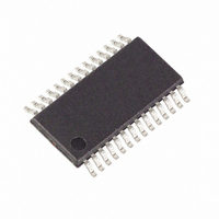
MAXQ3108-FFN+ Maxim Integrated Products, MAXQ3108-FFN+ Datasheet - Page 19

MAXQ3108-FFN+
Manufacturer Part Number
MAXQ3108-FFN+
Description
IC MCU DUAL-CORE 16BIT 28-TSSOP
Manufacturer
Maxim Integrated Products
Series
MAXQ™r
Datasheet
1.MAXQ3108-FFN.pdf
(64 pages)
Specifications of MAXQ3108-FFN+
Core Processor
RISC
Core Size
16-Bit
Speed
10MHz
Connectivity
I²C, SPI, UART/USART
Peripherals
POR, PWM, WDT
Number Of I /o
21
Program Memory Size
64KB (32K x 16)
Program Memory Type
FLASH
Ram Size
11K x 8
Voltage - Supply (vcc/vdd)
1.8 V ~ 3.6 V
Oscillator Type
External
Operating Temperature
-40°C ~ 85°C
Package / Case
28-TSSOP
Processor Series
MAXQ
Core
RISC
Data Bus Width
16 bit
Data Ram Size
2 KB
Interface Type
I2C, JTAG, SPI
Maximum Clock Frequency
10 MHz
Number Of Programmable I/os
22
Number Of Timers
2
Operating Supply Voltage
3.6 V
Maximum Operating Temperature
+ 85 C
Mounting Style
SMD/SMT
Minimum Operating Temperature
- 40 C
Lead Free Status / RoHS Status
Lead free / RoHS Compliant
Eeprom Size
-
Data Converters
-
Lead Free Status / Rohs Status
Lead free / RoHS Compliant
MREQ1 (0Fh, 00h)
Initialization:
Read/Write Access:
MREQ1.[15:0]:
MREQ2 (10h, 00h)
Initialization:
Read/Write Access:
MREQ2.[15:0]:
ADCN (11h, 00h)
Initialization:
Read/Write Access:
ADCN.0: ABF0
ADCN.1: ABF1
ADCN.2: ABF2
ADCN.3: ABF3
ADCN.4: ABF4
______________________________________________________________________________________
Low-Power, Dual-Core Microcontroller
Master Request Register 1
This register is reset to 0000h on all forms of reset.
Unrestricted read/write access only to the UserCore.
Unrestricted read access only to the DSPCore.
Master Request Register 1 Bits 15:0. These bits are used to supply follow-on address and data
information for commands issued by the master. To notify the slave that data is ready to be read,
the REQCDV bit should be set to 1. The master should poll the REQCDV bit to know when the slave
has read MREQ1 and when it is safe to write further data to MREQ1.
Master Request Register 2
This register is reset to 0000h on all forms of reset.
Unrestricted read/write access only to the UserCore.
Unrestricted read access only to the DSPCore.
Master Request Register 2 Bits 15:0. These bits are used to supply follow-on address and data
information for commands issued by the master. To notify the slave that data is ready to be read,
the REQCDV bit should be set to 1. The master should poll the REQCDV bit to know when the slave
has read MREQ2 and when it is safe to write further data to MREQ2.
Analog-to-Digital Converter Control Register
This register is cleared to 0000h on all forms of reset.
UserCore: Unrestricted read/write access except bits 0:5 are read only and 6:7 have hardware
restricted write access.
DSPCore: Read-only.
ADC0 Buffer Full Flag. This bit is set by hardware to indicate that a sample is available from
ADC0. An interrupt request is generated to a CPU if IF01E = 1 and interrupts are not otherwise
masked globally or modularly. This bit is cleared by hardware by a CPU read (either the UserCore
or the DSPCore) of the AD0 output register. The ABF0 and ABF1 flags are set in the same clock
cycle.
ADC1 Buffer Full Flag. This bit is set by hardware to indicate that a sample is available from
ADC1. An interrupt request is generated to a CPU if IF01E = 1 and interrupts are not otherwise
masked globally or modularly. This bit is cleared by hardware by a CPU read (either the UserCore
or the DSPCore) of the AD1 output register. The ABF0 and ABF1 flags are set in the same clock
cycle.
ADC2 Buffer Full Flag. This bit is set by hardware to indicate that a sample is available from
ADC2. An interrupt request is generated to a CPU if IF23E = 1 and interrupts are not otherwise
masked globally or modularly. This bit is cleared by hardware by a CPU read (either the UserCore
or the DSPCore) of the AD2 output register. The ABF2 and ABF3 flags are set in the same clock
cycle.
ADC3 Buffer Full Flag. This bit is set by hardware to indicate that a sample is available from
ADC3. An interrupt request is generated to a CPU if IF23E = 1 and interrupts are not otherwise
masked globally or modularly. This bit is cleared by hardware by a CPU read (either the UserCore
or the DSPCore) of the AD3 output register. The ABF2 and ABF3 flags are set in the same clock
cycle.
ADC4 Buffer Full Flag. This bit is set by hardware to indicate that a sample is available from
ADC4. An interrupt request is generated to a CPU if IF45E = 1 and interrupts are not otherwise
masked globally or modularly. This bit is cleared by hardware by a CPU read (either the UserCore
or the DSPCore) of the AD4 output register. The ABF4 and ABF5 flags are set in the same clock
cycle.
Special Function Register Bit Descriptions (continued)
19


