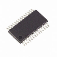
MAXQ3108-FFN+ Maxim Integrated Products, MAXQ3108-FFN+ Datasheet - Page 60

MAXQ3108-FFN+
Manufacturer Part Number
MAXQ3108-FFN+
Description
IC MCU DUAL-CORE 16BIT 28-TSSOP
Manufacturer
Maxim Integrated Products
Series
MAXQ™r
Datasheet
1.MAXQ3108-FFN.pdf
(64 pages)
Specifications of MAXQ3108-FFN+
Core Processor
RISC
Core Size
16-Bit
Speed
10MHz
Connectivity
I²C, SPI, UART/USART
Peripherals
POR, PWM, WDT
Number Of I /o
21
Program Memory Size
64KB (32K x 16)
Program Memory Type
FLASH
Ram Size
11K x 8
Voltage - Supply (vcc/vdd)
1.8 V ~ 3.6 V
Oscillator Type
External
Operating Temperature
-40°C ~ 85°C
Package / Case
28-TSSOP
Processor Series
MAXQ
Core
RISC
Data Bus Width
16 bit
Data Ram Size
2 KB
Interface Type
I2C, JTAG, SPI
Maximum Clock Frequency
10 MHz
Number Of Programmable I/os
22
Number Of Timers
2
Operating Supply Voltage
3.6 V
Maximum Operating Temperature
+ 85 C
Mounting Style
SMD/SMT
Minimum Operating Temperature
- 40 C
Lead Free Status / RoHS Status
Lead free / RoHS Compliant
Eeprom Size
-
Data Converters
-
Lead Free Status / Rohs Status
Lead free / RoHS Compliant
Low-Power, Dual-Core Microcontroller
DSPCore uses 8KB (4K instruction words) of RAM as
code memory, with a separate 1KB (512 word) data
space.
Code memory for the DSPCore is implemented as an
8KB block of static RAM. Following power-on reset, the
DSPCore CPU is disabled (that is, ENDSP is clear).
Since the DSPCore is not fetching instructions, its code
memory can be remapped to the UserCore data space.
The DSPCore code RAM is mapped into UserCore data
space at 0x1000–0x2FFF in byte mode (or
0x1000–0x1FFF in word mode).
Code for the DSPCore must be compiled along with the
code for the UserCore as an independent, self-con-
tained module. That is, the DSPCore code cannot con-
tain calls to modules in the UserCore and cannot
depend on any C runtime code that is executed only in
the UserCore. For this reason, it is likely that develop-
ment for the DSPCore is done in assembly language
rather than C. Code for the DSPCore must be compiled
to run at location 0x8000 and must be located in a seg-
ment with a known absolute address.
To configure DSP code memory at runtime using the
utility ROM copy routines:
• Establish a word array at location 0x1000.
• Establish a word pointer (DP[0]) at the start of the
• Add 0x8000 to DP[0].
• Call the utility ROM function UROM_moveDPinc.
• Copy the result to the word array and increment the
• Repeat until complete.
Once the copy is complete, setting the ENDSP bit relo-
cates the RAM block from 0x1000 in UserCore data
space to 0x8000 in DSPCore code space and releases
DSPCore reset. When DSPCore reset is released, the
DSPCore begins executing instructions from the RAM
block at 0x8000.
A set of five registers is used to communicate between
the UserCore and the DSPCore. Three registers,
MREQ0, MREQ1 and MREQ2, are dedicated to com-
municating requests from the UserCore to the
DSPCore; two registers, SRSP0 and SRSP1, manage
responses from the DSPCore to the UserCore.
The UserCore starts all communication between the two
cores. Typically, the UserCore and the DSPCore agree
on a set of 4-bit request codes that the DSPCore recog-
60
DSPCore code block in flash.
array pointer.
______________________________________________________________________________________
Intercore Communications
DSP Code Memory
nizes and to which it responds. For example, request
code 1 might be a software reset; request code 2 might
be a read RAM request; request code 3 might be a
write RAM request.
A set of hardware locks keep the two cores in synchro-
nization for purposes of communication. The REQCDV
(request command data valid) bit in the MREQ0 is set
by the UserCore to alert the DSPCore that a request is
pending. When the DSPCore has read the request, it
can clear the REQCDV bit. Only the DSPCore can clear
the bit; thus, coherency is guaranteed. Similarly, when
the DSPCore has a response available it sets the
RSPSDV (response status data valid). When the
UserCore has received the response data, it clears the
RSPSDV bit. Since only the DSPCore can set this bit
and only the UserCore can clear it, once again,
coherency is guaranteed.
A typical use-case scenario would proceed as follows.
Case 1: Load the 16-bit value 0x55AA to RAM loca-
tion 0x0020 in the DSPCore. It has been established
that the command for RAM write is 0x03.
1) The UserCore loads the 16-bit address 0x0020 into
2) The UserCore loads 0x23 into the MREQ0 register.
3) The DSPCore receives the alert that a command is
4) The DSPCore completes the RAM write operation.
5) The DSPCore then clears the REQCDV bit in the
Case 2: Read the 16-bit value at DSPCore RAM loca-
tion 0x0030. It has been established that the com-
mand for RAM read is 0x02.
1) The UserCore loads the 16-bit address 0x0030 into
2) The UserCore loads 0x22 into the MREQ0 register.
3) The DSPCore receives the alert that a command is
MREQ1 and the 16-bit data word 0x55AA into
MREQ2.
This simultaneously loads the command 0x03 into
the request command and sets the REQCDV bit to
alert the DSPCore that a command is pending.
pending and retrieves the command from the
MREQ0 register. It decodes the request as a RAM
write request (0x03.) In response, it reads MREQ1
for the address and MREQ2 for the data to write.
MREQ0 register to signal the successful execution
of the command.
MREQ1.
This action simultaneously loads the command
0x02 into the request command and sets the
REQCDV bit to alert the DSPCore that a command
is pending.
pending and retrieves the command from the


