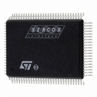
ST92F150JDV1QC STMicroelectronics, ST92F150JDV1QC Datasheet - Page 120

ST92F150JDV1QC
Manufacturer Part Number
ST92F150JDV1QC
Description
IC MCU 128K FLASH 100-PQFP
Manufacturer
STMicroelectronics
Series
ST9r
Datasheet
1.ST92F150CV1TB.pdf
(429 pages)
Specifications of ST92F150JDV1QC
Core Processor
ST9
Core Size
8/16-Bit
Speed
24MHz
Connectivity
CAN, I²C, LIN, SCI, SPI
Peripherals
DMA, LVD, POR, PWM, WDT
Number Of I /o
77
Program Memory Size
128KB (128K x 8)
Program Memory Type
FLASH
Eeprom Size
1K x 8
Ram Size
6K x 8
Voltage - Supply (vcc/vdd)
4.5 V ~ 5.5 V
Data Converters
A/D 16x10b
Oscillator Type
Internal
Operating Temperature
-40°C ~ 125°C
Package / Case
100-QFP
Processor Series
ST92F15x
Core
ST9
Data Bus Width
8 bit, 16 bit
Data Ram Size
6 KB
Interface Type
CAN, I2C, SCI, SPI
Maximum Clock Frequency
24 MHz
Number Of Programmable I/os
80
Number Of Timers
5 x 16 bit
Operating Supply Voltage
4.5 V to 5.5 V
Maximum Operating Temperature
+ 105 C
Mounting Style
SMD/SMT
Development Tools By Supplier
ST92F150-EPB
Minimum Operating Temperature
- 40 C
On-chip Adc
16 bit x 10 bit
Case
QFP
Lead Free Status / RoHS Status
Lead free / RoHS Compliant
Other names
497-2137
Available stocks
Company
Part Number
Manufacturer
Quantity
Price
- Current page: 120 of 429
- Download datasheet (8Mb)
ST92F124/F150/F250 - INTERRUPTS
WAKE-UP / INTERRUPT LINES MANAGEMENT UNIT (Cont’d)
WAKE-UP
(WUTRH)
R252 - Read/Write
Register Page: 57
Reset Value: 0000 0000 (00h)
Bit 7:0 = WUT[15:8]: Wake-Up Trigger Polarity
Bits
These bits are set and cleared by software.
0: The corresponding WUPx pending bit will be set
1: The corresponding WUPx pending bit will be set
WAKE-UP TRIGGER REGISTER LOW (WUTRL)
R253 - Read/Write
Register Page: 57
Reset Value: 0000 0000 (00h)
Bit 7:0 = WUT[7:0]: Wake-Up Trigger Polarity Bits
These bits are set and cleared by software.
0: The corresponding WUPx pending bit will be set
1: The corresponding WUPx pending bit will be set
WARNING
1. As the external wake-up lines are edge trig-
2. If either a rising or a falling edge on the external
120/429
WUT15 WUT14 WUT13 WUT12 WUT11 WUT10 WUT9
9
WUT7
on the falling edge of the input wake-up line .
on the rising edge of the input wake-up line.
on the falling edge of the input wake-up line.
on the rising edge of the input wake-up line.
gered, no glitches must be generated on these
lines.
wake-up
WUTRLH or WUTRL registers, the pending bit
will not be set.
7
7
WUT6
WUT5
lines
TRIGGER
WUT4
occurs
WUT3
REGISTER
while
WUT2
writing
WUT1
HIGH
WUT8
WUT0
0
0
the
WAKE-UP PENDING REGISTER HIGH
(WUPRH)
R254 - Read/Write
Register Page: 57
Reset Value: 0000 0000 (00h)
Bit 7:0 = WUP[15:8]: Wake-Up Pending Bits
These bits are set by hardware on occurrence of
the trigger event on the corresponding wake-up
line. They must be cleared by software. They can
be set by software to implement a software inter-
rupt.
0: No Wake-up Trigger event occurred
1: Wake-up Trigger event occured
WAKE-UP PENDING REGISTER LOW (WUPRL)
R255 - Read/Write
Register Page: 57
Reset Value: 0000 0000 (00h)
Bit 7:0 = WUP[7:0]: Wake-Up Pending Bits
These bits are set by hardware on occurrence of
the trigger event on the corresponding wake-up
line. They must be cleared by software. They can
be set by software to implement a software inter-
rupt.
0: No Wake-up Trigger event occurred
1: Wake-up Trigger event occured
Note: To avoid losing a trigger event while clear-
ing the pending bits, it is recommended to use
read-modify-write
BAND) to clear them.
5.12.6 Important Note On WUIMU
Refer to
WUP15 WUP14 WUP13 WUP12 WUP11 WUP10 WUP9
WUP7
7
7
WUP6
Section 13.2 on page
WUP5
instructions
WUP4
WUP3
409.
WUP2
(AND,
WUP1
BRES,
WUP8
WUP0
0
0
Related parts for ST92F150JDV1QC
Image
Part Number
Description
Manufacturer
Datasheet
Request
R

Part Number:
Description:
BOARD PROGRAM FOR ST92F150 MCU
Manufacturer:
STMicroelectronics
Datasheet:

Part Number:
Description:
BOARD EVALUATION FOR ST9 SERIES
Manufacturer:
STMicroelectronics
Datasheet:

Part Number:
Description:
BOARD EMULATOR FOR ST9 SERIES
Manufacturer:
STMicroelectronics
Datasheet:

Part Number:
Description:
MCU, MPU & DSP Development Tools ST9 Dedication Board
Manufacturer:
STMicroelectronics
Datasheet:

Part Number:
Description:
STMicroelectronics [RIPPLE-CARRY BINARY COUNTER/DIVIDERS]
Manufacturer:
STMicroelectronics
Datasheet:

Part Number:
Description:
STMicroelectronics [LIQUID-CRYSTAL DISPLAY DRIVERS]
Manufacturer:
STMicroelectronics
Datasheet:

Part Number:
Description:
BOARD EVAL FOR MEMS SENSORS
Manufacturer:
STMicroelectronics
Datasheet:

Part Number:
Description:
NPN TRANSISTOR POWER MODULE
Manufacturer:
STMicroelectronics
Datasheet:

Part Number:
Description:
TURBOSWITCH ULTRA-FAST HIGH VOLTAGE DIODE
Manufacturer:
STMicroelectronics
Datasheet:

Part Number:
Description:
Manufacturer:
STMicroelectronics
Datasheet:

Part Number:
Description:
DIODE / SCR MODULE
Manufacturer:
STMicroelectronics
Datasheet:

Part Number:
Description:
DIODE / SCR MODULE
Manufacturer:
STMicroelectronics
Datasheet:


