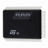
ST92F150JDV1QC STMicroelectronics, ST92F150JDV1QC Datasheet - Page 37

ST92F150JDV1QC
Manufacturer Part Number
ST92F150JDV1QC
Description
IC MCU 128K FLASH 100-PQFP
Manufacturer
STMicroelectronics
Series
ST9r
Datasheet
1.ST92F150CV1TB.pdf
(429 pages)
Specifications of ST92F150JDV1QC
Core Processor
ST9
Core Size
8/16-Bit
Speed
24MHz
Connectivity
CAN, I²C, LIN, SCI, SPI
Peripherals
DMA, LVD, POR, PWM, WDT
Number Of I /o
77
Program Memory Size
128KB (128K x 8)
Program Memory Type
FLASH
Eeprom Size
1K x 8
Ram Size
6K x 8
Voltage - Supply (vcc/vdd)
4.5 V ~ 5.5 V
Data Converters
A/D 16x10b
Oscillator Type
Internal
Operating Temperature
-40°C ~ 125°C
Package / Case
100-QFP
Processor Series
ST92F15x
Core
ST9
Data Bus Width
8 bit, 16 bit
Data Ram Size
6 KB
Interface Type
CAN, I2C, SCI, SPI
Maximum Clock Frequency
24 MHz
Number Of Programmable I/os
80
Number Of Timers
5 x 16 bit
Operating Supply Voltage
4.5 V to 5.5 V
Maximum Operating Temperature
+ 105 C
Mounting Style
SMD/SMT
Development Tools By Supplier
ST92F150-EPB
Minimum Operating Temperature
- 40 C
On-chip Adc
16 bit x 10 bit
Case
QFP
Lead Free Status / RoHS Status
Lead free / RoHS Compliant
Other names
497-2137
Available stocks
Company
Part Number
Manufacturer
Quantity
Price
- Current page: 37 of 429
- Download datasheet (8Mb)
SYSTEM REGISTERS (Cont’d)
POINTER 0 REGISTER (RP0)
R232 - Read/Write
Register Group: E (System)
Reset Value: xxxx xx00 (xxh)
Bits 7:3 = RG[4:0]: Register Group number.
These bits contain the number (in the range 0 to
31) of the register block specified in the srp0 or
srp instructions. In single 16-register mode the
number indicates the lower of the two 8-register
blocks to which the 16 working registers are to be
mapped, while in twin 8-register mode it indicates
the 8-register block to which r0 to r7 are to be
mapped.
Bit 2 = RPS: Register Pointer Selector.
This bit is set by the instructions srp0 and srp1 to
indicate that the twin register pointing mode is se-
lected. The bit is reset by the srp instruction to in-
dicate that the single register pointing mode is se-
lected.
0: Single register pointing mode
1: Twin register pointing mode
Bits 1:0: Reserved. Forced by hardware to zero.
RG4
7
RG3
RG2
RG1
RG0
RPS
0
0
0
ST92F124/F150/F250 - DEVICE ARCHITECTURE
POINTER 1 REGISTER (RP1)
R233 - Read/Write
Register Group: E (System)
Reset Value: xxxx xx00 (xxh)
This register is only used in the twin register point-
ing mode. When using the single register pointing
mode, or when using only one of the twin register
groups, the RP1 register must be considered as
RESERVED and may NOT be used as a general
purpose register.
Bits 7:3 = RG[4:0]: Register Group number.
These bits contain the number (in the range 0 to
31) of the 8-register block specified in the srp1 in-
struction, to which r8 to r15 are to be mapped.
Bit 2 = RPS: Register Pointer Selector.
This bit is set by the srp0 and srp1 instructions to
indicate that the twin register pointing mode is se-
lected. The bit is reset by the srp instruction to in-
dicate that the single register pointing mode is se-
lected.
0: Single register pointing mode
1: Twin register pointing mode
Bits 1:0: Reserved. Forced by hardware to zero.
RG4
7
RG3
RG2
RG1
RG0
RPS
0
37/429
0
0
9
Related parts for ST92F150JDV1QC
Image
Part Number
Description
Manufacturer
Datasheet
Request
R

Part Number:
Description:
BOARD PROGRAM FOR ST92F150 MCU
Manufacturer:
STMicroelectronics
Datasheet:

Part Number:
Description:
BOARD EVALUATION FOR ST9 SERIES
Manufacturer:
STMicroelectronics
Datasheet:

Part Number:
Description:
BOARD EMULATOR FOR ST9 SERIES
Manufacturer:
STMicroelectronics
Datasheet:

Part Number:
Description:
MCU, MPU & DSP Development Tools ST9 Dedication Board
Manufacturer:
STMicroelectronics
Datasheet:

Part Number:
Description:
STMicroelectronics [RIPPLE-CARRY BINARY COUNTER/DIVIDERS]
Manufacturer:
STMicroelectronics
Datasheet:

Part Number:
Description:
STMicroelectronics [LIQUID-CRYSTAL DISPLAY DRIVERS]
Manufacturer:
STMicroelectronics
Datasheet:

Part Number:
Description:
BOARD EVAL FOR MEMS SENSORS
Manufacturer:
STMicroelectronics
Datasheet:

Part Number:
Description:
NPN TRANSISTOR POWER MODULE
Manufacturer:
STMicroelectronics
Datasheet:

Part Number:
Description:
TURBOSWITCH ULTRA-FAST HIGH VOLTAGE DIODE
Manufacturer:
STMicroelectronics
Datasheet:

Part Number:
Description:
Manufacturer:
STMicroelectronics
Datasheet:

Part Number:
Description:
DIODE / SCR MODULE
Manufacturer:
STMicroelectronics
Datasheet:

Part Number:
Description:
DIODE / SCR MODULE
Manufacturer:
STMicroelectronics
Datasheet:


