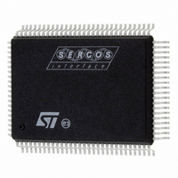
ST92F150JDV1QC STMicroelectronics, ST92F150JDV1QC Datasheet - Page 208

ST92F150JDV1QC
Manufacturer Part Number
ST92F150JDV1QC
Description
IC MCU 128K FLASH 100-PQFP
Manufacturer
STMicroelectronics
Series
ST9r
Datasheet
1.ST92F150CV1TB.pdf
(429 pages)
Specifications of ST92F150JDV1QC
Core Processor
ST9
Core Size
8/16-Bit
Speed
24MHz
Connectivity
CAN, I²C, LIN, SCI, SPI
Peripherals
DMA, LVD, POR, PWM, WDT
Number Of I /o
77
Program Memory Size
128KB (128K x 8)
Program Memory Type
FLASH
Eeprom Size
1K x 8
Ram Size
6K x 8
Voltage - Supply (vcc/vdd)
4.5 V ~ 5.5 V
Data Converters
A/D 16x10b
Oscillator Type
Internal
Operating Temperature
-40°C ~ 125°C
Package / Case
100-QFP
Processor Series
ST92F15x
Core
ST9
Data Bus Width
8 bit, 16 bit
Data Ram Size
6 KB
Interface Type
CAN, I2C, SCI, SPI
Maximum Clock Frequency
24 MHz
Number Of Programmable I/os
80
Number Of Timers
5 x 16 bit
Operating Supply Voltage
4.5 V to 5.5 V
Maximum Operating Temperature
+ 105 C
Mounting Style
SMD/SMT
Development Tools By Supplier
ST92F150-EPB
Minimum Operating Temperature
- 40 C
On-chip Adc
16 bit x 10 bit
Case
QFP
Lead Free Status / RoHS Status
Lead free / RoHS Compliant
Other names
497-2137
Available stocks
Company
Part Number
Manufacturer
Quantity
Price
- Current page: 208 of 429
- Download datasheet (8Mb)
MULTIFUNCTION TIMER (MFT)
MULTIFUNCTION TIMER (Cont’d)
FLAG REGISTER (T_FLAGR)
R254 - Read/Write
Register Page: 10
Reset value: 0000 0000 (00h)
Bit 7 = CP0: Capture 0 flag.
This bit is set by hardware after a capture on
REG0R register. An interrupt is generated de-
pending on the value of the GTIEN, CP0I bits in
the IDMR register and the A0 bit in the T_FLAGR
register. The CP0 bit must be cleared by software.
Setting by software acts as a software load/cap-
ture to/from the REG0R register.
0: No Capture 0 event
1: Capture 0 event occurred
Bit 6 = CP1: Capture 1 flag.
This bit is set by hardware after a capture on
REG1R register. An interrupt is generated de-
pending on the value of the GTIEN, CP0I bits in
the IDMR register and the A0 bit in the T_FLAGR
register. The CP1 bit must be cleared by software.
Setting by software acts as a capture event on the
REG1R register, except when in Bicapture mode.
0: No Capture 1 event
1: Capture 1 event occurred
Bit 5 = CM0: Compare 0 flag.
This bit is set by hardware after a successful com-
pare on the CMP0R register. An interrupt is gener-
ated if the GTIEN and CM0I bits in the IDMR reg-
ister are set. The CM0 bit is cleared by software.
0: No Compare 0 event
1: Compare 0 event occurred
Bit 4 = CM1: Compare 1 flag.
This bit is set after a successful compare on
CMP1R register. An interrupt is generated if the
208/429
9
CP0 CP1 CM0 CM1 OUF
7
OCP0
OCM0 A0
0
GTIEN and CM1I bits in the IDMR register are set.
The CM1 bit is cleared by software.
0: No Compare 1 event
1: Compare 1 event occurred
Bit 3 = OUF: Overflow/Underflow.
This bit is set by hardware after a counter Over/
Underflow condition. An interrupt is generated if
GTIEN and OUI=1 in the IDMR register. The OUF
bit is cleared by software.
0: No counter overflow/underflow
1: Counter overflow/underflow
Bit 2 = OCP0: Overrun on Capture 0.
This bit is set by hardware when more than one
INT/DMA requests occur before the CP0 flag is
cleared by software or whenever a capture is sim-
ulated by setting the CP0 flag by software. The
OCP0 flag is cleared by software.
0: No capture 0 overrun
1: Capture 0 overrun
Bit 1 = OCM0: Overrun on compare 0.
This bit is set by hardware when more than one
INT/DMA requests occur before the CM0 flag is
cleared by software.The OCM0 flag is cleared by
software.
0: No compare 0 overrun
1: Compare 0 overrun
Bit 0 = A0: Capture interrupt function.
This bit is set and cleared by software.
0: Configure the capture interrupt as an OR func-
1: Configure the capture interrupt as an AND func-
Note: When A0 is set, both CP0I and CP1I in the
IDMR register must be set to enable both capture
interrupts.
tion of REG0R/REG1R captures
tion of REG0R/REG1R captures
Related parts for ST92F150JDV1QC
Image
Part Number
Description
Manufacturer
Datasheet
Request
R

Part Number:
Description:
BOARD PROGRAM FOR ST92F150 MCU
Manufacturer:
STMicroelectronics
Datasheet:

Part Number:
Description:
BOARD EVALUATION FOR ST9 SERIES
Manufacturer:
STMicroelectronics
Datasheet:

Part Number:
Description:
BOARD EMULATOR FOR ST9 SERIES
Manufacturer:
STMicroelectronics
Datasheet:

Part Number:
Description:
MCU, MPU & DSP Development Tools ST9 Dedication Board
Manufacturer:
STMicroelectronics
Datasheet:

Part Number:
Description:
STMicroelectronics [RIPPLE-CARRY BINARY COUNTER/DIVIDERS]
Manufacturer:
STMicroelectronics
Datasheet:

Part Number:
Description:
STMicroelectronics [LIQUID-CRYSTAL DISPLAY DRIVERS]
Manufacturer:
STMicroelectronics
Datasheet:

Part Number:
Description:
BOARD EVAL FOR MEMS SENSORS
Manufacturer:
STMicroelectronics
Datasheet:

Part Number:
Description:
NPN TRANSISTOR POWER MODULE
Manufacturer:
STMicroelectronics
Datasheet:

Part Number:
Description:
TURBOSWITCH ULTRA-FAST HIGH VOLTAGE DIODE
Manufacturer:
STMicroelectronics
Datasheet:

Part Number:
Description:
Manufacturer:
STMicroelectronics
Datasheet:

Part Number:
Description:
DIODE / SCR MODULE
Manufacturer:
STMicroelectronics
Datasheet:

Part Number:
Description:
DIODE / SCR MODULE
Manufacturer:
STMicroelectronics
Datasheet:


