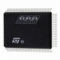
ST92F150JDV1QC STMicroelectronics, ST92F150JDV1QC Datasheet - Page 253

ST92F150JDV1QC
Manufacturer Part Number
ST92F150JDV1QC
Description
IC MCU 128K FLASH 100-PQFP
Manufacturer
STMicroelectronics
Series
ST9r
Datasheet
1.ST92F150CV1TB.pdf
(429 pages)
Specifications of ST92F150JDV1QC
Core Processor
ST9
Core Size
8/16-Bit
Speed
24MHz
Connectivity
CAN, I²C, LIN, SCI, SPI
Peripherals
DMA, LVD, POR, PWM, WDT
Number Of I /o
77
Program Memory Size
128KB (128K x 8)
Program Memory Type
FLASH
Eeprom Size
1K x 8
Ram Size
6K x 8
Voltage - Supply (vcc/vdd)
4.5 V ~ 5.5 V
Data Converters
A/D 16x10b
Oscillator Type
Internal
Operating Temperature
-40°C ~ 125°C
Package / Case
100-QFP
Processor Series
ST92F15x
Core
ST9
Data Bus Width
8 bit, 16 bit
Data Ram Size
6 KB
Interface Type
CAN, I2C, SCI, SPI
Maximum Clock Frequency
24 MHz
Number Of Programmable I/os
80
Number Of Timers
5 x 16 bit
Operating Supply Voltage
4.5 V to 5.5 V
Maximum Operating Temperature
+ 105 C
Mounting Style
SMD/SMT
Development Tools By Supplier
ST92F150-EPB
Minimum Operating Temperature
- 40 C
On-chip Adc
16 bit x 10 bit
Case
QFP
Lead Free Status / RoHS Status
Lead free / RoHS Compliant
Other names
497-2137
Available stocks
Company
Part Number
Manufacturer
Quantity
Price
- Current page: 253 of 429
- Download datasheet (8Mb)
SERIAL PERIPHERAL INTERFACE (Cont’d)
10.7.4.2 Slave Configuration
In slave configuration, the serial clock is received
on the SCK pin from the master device.
The value of the SPPR register and SPR0 & SPR1
bits in the SPCR is not used for the data transfer.
Procedure
In this configuration the MOSI pin is a data input
and the MISO pin is a data output.
Transmit Sequence
The data byte is parallel loaded into the 8-bit shift
register (from the internal bus) during a write cycle
and then shifted out serially to the MISO pin most
significant bit first.
The transmit sequence begins when the slave de-
vice receives the clock signal and the most signifi-
cant bit of the data on its MOSI pin.
– For correct data transfer, the slave device
– The SS pin must be connected to a low level
– Clear the MSTR bit and set the SPOE bit to
must be in the same timing mode as the mas-
ter device (CPOL and CPHA bits). See
123.
signal during the complete byte transmit se-
quence.
assign the pins to alternate function.
Figure
When data transfer is complete:
During the last clock cycle the SPIF bit is set, a
copy of the data byte received in the shift register
is moved to a buffer. When the SPDR register is
read, the SPI peripheral returns this buffered val-
ue.
Clearing the SPIF bit is performed by the following
software sequence:
1. An access to the SPSR register while the SPIF
2. A read of the SPDR register.
Notes: While the SPIF bit is set, all writes to the
SPDR register are inhibited until the SPSR regis-
ter is read.
The SPIF bit can be cleared during a second
transmission; however, it must be cleared before
the second SPIF bit in order to prevent an overrun
condition (see
Depending on the CPHA bit, the SS pin has to be
set to write to the SPDR register between each
data byte transfer to avoid a write collision (see
Section
SERIAL PERIPHERAL INTERFACE (SPI)
– The SPIF bit is set by hardware
– An interrupt is generated if the SPIS and SPIE
bit is set.
bits are set.
10.7.4.4).
Section
10.7.4.6).
253/429
9
Related parts for ST92F150JDV1QC
Image
Part Number
Description
Manufacturer
Datasheet
Request
R

Part Number:
Description:
BOARD PROGRAM FOR ST92F150 MCU
Manufacturer:
STMicroelectronics
Datasheet:

Part Number:
Description:
BOARD EVALUATION FOR ST9 SERIES
Manufacturer:
STMicroelectronics
Datasheet:

Part Number:
Description:
BOARD EMULATOR FOR ST9 SERIES
Manufacturer:
STMicroelectronics
Datasheet:

Part Number:
Description:
MCU, MPU & DSP Development Tools ST9 Dedication Board
Manufacturer:
STMicroelectronics
Datasheet:

Part Number:
Description:
STMicroelectronics [RIPPLE-CARRY BINARY COUNTER/DIVIDERS]
Manufacturer:
STMicroelectronics
Datasheet:

Part Number:
Description:
STMicroelectronics [LIQUID-CRYSTAL DISPLAY DRIVERS]
Manufacturer:
STMicroelectronics
Datasheet:

Part Number:
Description:
BOARD EVAL FOR MEMS SENSORS
Manufacturer:
STMicroelectronics
Datasheet:

Part Number:
Description:
NPN TRANSISTOR POWER MODULE
Manufacturer:
STMicroelectronics
Datasheet:

Part Number:
Description:
TURBOSWITCH ULTRA-FAST HIGH VOLTAGE DIODE
Manufacturer:
STMicroelectronics
Datasheet:

Part Number:
Description:
Manufacturer:
STMicroelectronics
Datasheet:

Part Number:
Description:
DIODE / SCR MODULE
Manufacturer:
STMicroelectronics
Datasheet:

Part Number:
Description:
DIODE / SCR MODULE
Manufacturer:
STMicroelectronics
Datasheet:


