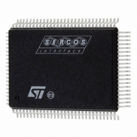
ST92F150JDV1QC STMicroelectronics, ST92F150JDV1QC Datasheet - Page 261

ST92F150JDV1QC
Manufacturer Part Number
ST92F150JDV1QC
Description
IC MCU 128K FLASH 100-PQFP
Manufacturer
STMicroelectronics
Series
ST9r
Datasheet
1.ST92F150CV1TB.pdf
(429 pages)
Specifications of ST92F150JDV1QC
Core Processor
ST9
Core Size
8/16-Bit
Speed
24MHz
Connectivity
CAN, I²C, LIN, SCI, SPI
Peripherals
DMA, LVD, POR, PWM, WDT
Number Of I /o
77
Program Memory Size
128KB (128K x 8)
Program Memory Type
FLASH
Eeprom Size
1K x 8
Ram Size
6K x 8
Voltage - Supply (vcc/vdd)
4.5 V ~ 5.5 V
Data Converters
A/D 16x10b
Oscillator Type
Internal
Operating Temperature
-40°C ~ 125°C
Package / Case
100-QFP
Processor Series
ST92F15x
Core
ST9
Data Bus Width
8 bit, 16 bit
Data Ram Size
6 KB
Interface Type
CAN, I2C, SCI, SPI
Maximum Clock Frequency
24 MHz
Number Of Programmable I/os
80
Number Of Timers
5 x 16 bit
Operating Supply Voltage
4.5 V to 5.5 V
Maximum Operating Temperature
+ 105 C
Mounting Style
SMD/SMT
Development Tools By Supplier
ST92F150-EPB
Minimum Operating Temperature
- 40 C
On-chip Adc
16 bit x 10 bit
Case
QFP
Lead Free Status / RoHS Status
Lead free / RoHS Compliant
Other names
497-2137
Available stocks
Company
Part Number
Manufacturer
Quantity
Price
- Current page: 261 of 429
- Download datasheet (8Mb)
SERIAL PERIPHERAL INTERFACE (Cont’d)
STATUS REGISTER (SPSR)
R242 - Read Only
Register Page: 7
Reset Value: 0000 0000 (00h)
Bit 7 = SPIF Serial Peripheral data transfer flag.
This bit is set by hardware when a transfer has
been completed. An interrupt is generated if
SPIE=1 in the SPCR register. It is cleared by a soft-
ware sequence (an access to the SPSR register
followed by a read or write to the SPDR register).
0: Data transfer is in progress or has been ap-
1: Data transfer between the device and an exter-
Note: While the SPIF bit is set, all writes to the
SPDR register are inhibited.
Bit 6 = WCOL Write Collision status.
This bit is set by hardware when a write to the
SPDR register is done during a transmit se-
quence. It is cleared by a software sequence (see
Figure
0: No write collision occurred
1: A write collision has been detected
Bit 5 = Unused.
Bit 4 = MODF Mode Fault flag.
This bit is set by hardware when the SS pin is
pulled low in master mode (see
Master Mode
erated if SPIE=1 in the SPCR register. This bit is
cleared by a software sequence (An access to the
SPSR register while MODF=1 followed by a write
to the SPCR register).
0: No master mode fault detected
SPIF
proved by a clearing sequence.
nal device has been completed.
7
124).
WCOL
Fault). An SPI interrupt can be gen-
-
MODF
-
Section 10.7.4.5
-
-
0
-
1: A fault in master mode has been detected
Bits 3:0 = Unused.
PRESCALER REGISTER (SPPR)
R243 - Read/Write
Register Page: 7
Reset Value: 0000 0000 (00h)
Bits 7:5 = Reserved, forced by hardware to 0.
Bit 4 = DIV2 Divider enable.
This bit is set and cleared by software.
0: Divider by 2 enabled.
1: Divider by 2 disabled.
Bit 3 = Reserved. forced by hardware to 0.
Bits 2:0 = PRS[2:0] Prescaler Value.
These bits are set and cleared by software. The
baud rate generator is driven by
INTCLK/(n1*n2*n3) where n1= PRS[2:0]+1, n2 is
the value defined by the SPR[1:0] bits (refer to
ble 49
DIV2=0. Refer to
These bits have no effect in slave mode.
Table 50. Prescaler Baud Rate
SERIAL PERIPHERAL INTERFACE (SPI)
7
0
Division Factor
1 (no division)
Prescaler
and
0
...
2
8
Table
0
50), n3 = 1 if DIV2=1 and n3= 2 if
Figure
DIV2
PRS2
121.
0
0
1
0
PRS2
PRS1
0
0
1
PRS1
PRS0
261/429
0
1
1
PRS0
Ta-
9
0
Related parts for ST92F150JDV1QC
Image
Part Number
Description
Manufacturer
Datasheet
Request
R

Part Number:
Description:
BOARD PROGRAM FOR ST92F150 MCU
Manufacturer:
STMicroelectronics
Datasheet:

Part Number:
Description:
BOARD EVALUATION FOR ST9 SERIES
Manufacturer:
STMicroelectronics
Datasheet:

Part Number:
Description:
BOARD EMULATOR FOR ST9 SERIES
Manufacturer:
STMicroelectronics
Datasheet:

Part Number:
Description:
MCU, MPU & DSP Development Tools ST9 Dedication Board
Manufacturer:
STMicroelectronics
Datasheet:

Part Number:
Description:
STMicroelectronics [RIPPLE-CARRY BINARY COUNTER/DIVIDERS]
Manufacturer:
STMicroelectronics
Datasheet:

Part Number:
Description:
STMicroelectronics [LIQUID-CRYSTAL DISPLAY DRIVERS]
Manufacturer:
STMicroelectronics
Datasheet:

Part Number:
Description:
BOARD EVAL FOR MEMS SENSORS
Manufacturer:
STMicroelectronics
Datasheet:

Part Number:
Description:
NPN TRANSISTOR POWER MODULE
Manufacturer:
STMicroelectronics
Datasheet:

Part Number:
Description:
TURBOSWITCH ULTRA-FAST HIGH VOLTAGE DIODE
Manufacturer:
STMicroelectronics
Datasheet:

Part Number:
Description:
Manufacturer:
STMicroelectronics
Datasheet:

Part Number:
Description:
DIODE / SCR MODULE
Manufacturer:
STMicroelectronics
Datasheet:

Part Number:
Description:
DIODE / SCR MODULE
Manufacturer:
STMicroelectronics
Datasheet:


