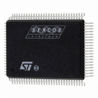
ST92F150JDV1QC STMicroelectronics, ST92F150JDV1QC Datasheet - Page 353

ST92F150JDV1QC
Manufacturer Part Number
ST92F150JDV1QC
Description
IC MCU 128K FLASH 100-PQFP
Manufacturer
STMicroelectronics
Series
ST9r
Datasheet
1.ST92F150CV1TB.pdf
(429 pages)
Specifications of ST92F150JDV1QC
Core Processor
ST9
Core Size
8/16-Bit
Speed
24MHz
Connectivity
CAN, I²C, LIN, SCI, SPI
Peripherals
DMA, LVD, POR, PWM, WDT
Number Of I /o
77
Program Memory Size
128KB (128K x 8)
Program Memory Type
FLASH
Eeprom Size
1K x 8
Ram Size
6K x 8
Voltage - Supply (vcc/vdd)
4.5 V ~ 5.5 V
Data Converters
A/D 16x10b
Oscillator Type
Internal
Operating Temperature
-40°C ~ 125°C
Package / Case
100-QFP
Processor Series
ST92F15x
Core
ST9
Data Bus Width
8 bit, 16 bit
Data Ram Size
6 KB
Interface Type
CAN, I2C, SCI, SPI
Maximum Clock Frequency
24 MHz
Number Of Programmable I/os
80
Number Of Timers
5 x 16 bit
Operating Supply Voltage
4.5 V to 5.5 V
Maximum Operating Temperature
+ 105 C
Mounting Style
SMD/SMT
Development Tools By Supplier
ST92F150-EPB
Minimum Operating Temperature
- 40 C
On-chip Adc
16 bit x 10 bit
Case
QFP
Lead Free Status / RoHS Status
Lead free / RoHS Compliant
Other names
497-2137
Available stocks
Company
Part Number
Manufacturer
Quantity
Price
- Current page: 353 of 429
- Download datasheet (8Mb)
CONTROLLER AREA NETWORK (Cont’d)
10.10.8.3 CAN Filter Registers
CAN FILTER CONFIGURATION REG.0 (CFCR0)
All bits of this register are set and cleared by soft-
ware.
Read / Write
Reset Value: 0000 0000 (00h)
Note: To modify the FFAx and FSCx bits, the bx-
CAN must be in INIT mode.
Bit 7 = FFA1 Filter FIFO Assignment for Filter 1
The message passing through this filter will be
stored in the specified FIFO.
0: Filter assigned to FIFO 0
1: Filter assigned to FIFO 1
Bit 6:5 = FSC1[1:0] Filter Scale Configuration
These bits define the scale configuration of Filter
1.
Bit 4 = FACT1 Filter Active
The software sets this bit to activate Filter 1. To
modify the Filter 1 registers (CF1R[7:0]), the
FACT1 bit must be cleared.
0: Filter 1 is not active
1: Filter 1 is active
Bit 3 = FFA0 Filter FIFO Assignment for Filter 0
The message passing through this filter will be
stored in the specified FIFO.
0: Filter assigned to FIFO 0
1: Filter assigned to FIFO 1
Bit 2:1 = FSC0[1:0] Filter Scale Configuration
These bits define the scale configuration of Filter
0.
Bit 0 = FACT0 Filter Active
The software sets this bit to activate Filter 0. To
modify the Filter 0 registers (CF0R[0:7]), the
FACT0 bit must be cleared.
0: Filter 0 is not active
1: Filter 0 is active
FFA1 FSC11 FSC10 FACT1 FFA0 FSC01 FSC00 FACT0
7
0
CONTROLLER AREA NETWORK (bxCAN)
CAN FILTER CONFIGURATION REG.1 (CFCR1)
All bits of this register are set and cleared by soft-
ware.
Read / Write
Reset Value: 0000 0000 (00h)
Bit 7 = FFA3 Filter FIFO Assignment for Filter 3
The message passing through this filter will be
stored in the specified FIFO.
0: Filter assigned to FIFO 0
1: Filter assigned to FIFO 1
Bit 6:5 = FSC3[1:0] Filter Scale Configuration
These bits define the scale configuration of Filter
3.
Bit 4 = FACT3 Filter Active
The software sets this bit to activate filter 3. To
modify the Filter 3 registers (CF3R[0:7]) the
FACT3 bit must be cleared.
0: Filter 3 is not active
1: Filter 3 is active
Bit 3 = FFA2 Filter FIFO Assignment for Filter 2
The message passing through this filter will be
stored in the specified FIFO.
0: Filter assigned to FIFO 0
1: Filter assigned to FIFO 1
Bit 2:1 = FSC2[1:0] Filter Scale Configuration
These bits define the scale configuration of Filter
2.
Bit 0 = FACT2 Filter Active
The software sets this bit to activate Filter 2. To
modify the Filter 2 registers (CF2R[0:7]), the
FACT2 bit must be cleared.
0: Filter 2 is not active
1: Filter 2 is active
FFA3 FSC31 FSC30 FACT3 FFA2 FSC21 FSC20 FACT2
7
353/429
0
9
Related parts for ST92F150JDV1QC
Image
Part Number
Description
Manufacturer
Datasheet
Request
R

Part Number:
Description:
BOARD PROGRAM FOR ST92F150 MCU
Manufacturer:
STMicroelectronics
Datasheet:

Part Number:
Description:
BOARD EVALUATION FOR ST9 SERIES
Manufacturer:
STMicroelectronics
Datasheet:

Part Number:
Description:
BOARD EMULATOR FOR ST9 SERIES
Manufacturer:
STMicroelectronics
Datasheet:

Part Number:
Description:
MCU, MPU & DSP Development Tools ST9 Dedication Board
Manufacturer:
STMicroelectronics
Datasheet:

Part Number:
Description:
STMicroelectronics [RIPPLE-CARRY BINARY COUNTER/DIVIDERS]
Manufacturer:
STMicroelectronics
Datasheet:

Part Number:
Description:
STMicroelectronics [LIQUID-CRYSTAL DISPLAY DRIVERS]
Manufacturer:
STMicroelectronics
Datasheet:

Part Number:
Description:
BOARD EVAL FOR MEMS SENSORS
Manufacturer:
STMicroelectronics
Datasheet:

Part Number:
Description:
NPN TRANSISTOR POWER MODULE
Manufacturer:
STMicroelectronics
Datasheet:

Part Number:
Description:
TURBOSWITCH ULTRA-FAST HIGH VOLTAGE DIODE
Manufacturer:
STMicroelectronics
Datasheet:

Part Number:
Description:
Manufacturer:
STMicroelectronics
Datasheet:

Part Number:
Description:
DIODE / SCR MODULE
Manufacturer:
STMicroelectronics
Datasheet:

Part Number:
Description:
DIODE / SCR MODULE
Manufacturer:
STMicroelectronics
Datasheet:


