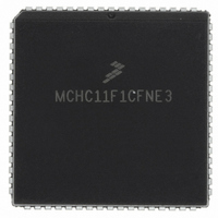
MCHC11F1CFNE3 Freescale Semiconductor, MCHC11F1CFNE3 Datasheet - Page 30

MCHC11F1CFNE3
Manufacturer Part Number
MCHC11F1CFNE3
Description
IC MCU 8BIT 1K RAM 68-PLCC
Manufacturer
Freescale Semiconductor
Series
HC11r
Specifications of MCHC11F1CFNE3
Core Processor
HC11
Core Size
8-Bit
Speed
3MHz
Connectivity
SCI, SPI
Peripherals
POR, WDT
Number Of I /o
30
Program Memory Type
ROMless
Eeprom Size
512 x 8
Ram Size
1K x 8
Voltage - Supply (vcc/vdd)
4.75 V ~ 5.25 V
Data Converters
A/D 8x8b
Oscillator Type
Internal
Operating Temperature
-40°C ~ 85°C
Package / Case
68-PLCC
A/d Inputs
8-Channel, 8-Bit
Eeprom Memory
512 Bytes
Input Output
30
Interface
SCI/SPI
Memory Type
EPROM
Number Of Bits
8
Package Type
68-pin PLCC
Programmable Memory
0 Bytes
Timers
3-16-bit
Voltage, Range
3-5.5 V
Controller Family/series
68HC11
No. Of I/o's
30
Eeprom Memory Size
512Byte
Ram Memory Size
1KB
Cpu Speed
3MHz
No. Of Timers
1
Embedded Interface Type
SCI, SPI
Rohs Compliant
Yes
Processor Series
HC11F
Core
HC11
Data Bus Width
8 bit
Program Memory Size
512 B
Data Ram Size
1 KB
Interface Type
SCI, SPI
Maximum Clock Frequency
3 MHz
Number Of Timers
1
Maximum Operating Temperature
+ 85 C
Mounting Style
SMD/SMT
Minimum Operating Temperature
- 40 C
On-chip Adc
8 bit, 8 Channel
Lead Free Status / RoHS Status
Lead free / RoHS Compliant
Program Memory Size
-
Lead Free Status / Rohs Status
RoHS Compliant part
Available stocks
Company
Part Number
Manufacturer
Quantity
Price
Company:
Part Number:
MCHC11F1CFNE3
Manufacturer:
FREESCALE
Quantity:
5 530
Company:
Part Number:
MCHC11F1CFNE3
Manufacturer:
FREESCALE
Quantity:
5 530
Company:
Part Number:
MCHC11F1CFNE3
Manufacturer:
Freescale Semiconductor
Quantity:
10 000
Company:
Part Number:
MCHC11F1CFNE3R
Manufacturer:
Freescale Semiconductor
Quantity:
10 000
ODD — Program Odd Rows (TEST)
EVEN — Program Even Rows (TEST)
ROW and BYTE — Row Erase Select Bit and Byte Erase Select
ERASE — Erase/Normal Control for EEPROM
EELAT — EEPROM Latch Control
EEPGM — EEPROM Program Command
EE[3:0] — EEPROM Map Position
Bit 3 — Not implemented. Reads always return one and writes have no effect.
NOCOP — COP System Disable
30
PPROG — EEPROM Programming Control
CONFIG — EEPROM Mapping, COP, EEPROM Enables
RESET
RESET
The value of these bits determines the manner in which EEPROM is erased. Bit encodings are shown
in 6.2 EEPROM Registers, page 30.
U = Unaffected by reset.
The CONFIG register is used to assign EEPROM a location in the memory map and to enable or disable
EEPROM operation. Bits in this register are user-programmed except when forced to certain values, as
noted in the following bit descriptions.
EEPROM is located at $xE00 – $xFFF, where x is the value represented by these four bits. In single-
chip and bootstrap modes, EEPROM is forced to $FE00 – $FFFF, regardless of the state of these bits.
On factory-fresh devices, EE[3:0] = $0.
0 = Normal read or program mode
1 = Erase mode
0 = EEPROM address and data bus configured for normal reads
1 = EEPROM address and data bus configured for programming or erasing
0 = Program or erase voltage to EEPROM array switched off
1 = Program or erase voltage to EEPROM array switched on
0 = COP enabled (forces reset on time-out)
1 = COP disabled (does not force reset on time-out)
ODD
Bit 7
Bit 7
EE3
U
0
EVEN
EE2
U
6
0
6
Freescale Semiconductor, Inc.
BYTE
For More Information On This Product,
0
0
1
1
Table 15 ROW and BYTE Encodings
EE1
U
5
0
0
5
Go to: www.freescale.com
BYTE
EE0
ROW
U
4
0
4
0
1
0
1
ROW
Bulk Erase (All 512 Bytes)
3
0
3
1
1
Row Erase (16 Bytes)
Byte Erase
Byte Erase
NOCOP
ERASE
Action
U
2
0
2
EELAT
1
0
1
1
1
EEPGM
EEON
MC68HC11F1/FC0
Bit 0
Bit 0
MC68HC11FTS/D
U
0
$x03B
$x03F


