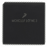
MCHC11F1CFNE3 Freescale Semiconductor, MCHC11F1CFNE3 Datasheet - Page 34

MCHC11F1CFNE3
Manufacturer Part Number
MCHC11F1CFNE3
Description
IC MCU 8BIT 1K RAM 68-PLCC
Manufacturer
Freescale Semiconductor
Series
HC11r
Specifications of MCHC11F1CFNE3
Core Processor
HC11
Core Size
8-Bit
Speed
3MHz
Connectivity
SCI, SPI
Peripherals
POR, WDT
Number Of I /o
30
Program Memory Type
ROMless
Eeprom Size
512 x 8
Ram Size
1K x 8
Voltage - Supply (vcc/vdd)
4.75 V ~ 5.25 V
Data Converters
A/D 8x8b
Oscillator Type
Internal
Operating Temperature
-40°C ~ 85°C
Package / Case
68-PLCC
A/d Inputs
8-Channel, 8-Bit
Eeprom Memory
512 Bytes
Input Output
30
Interface
SCI/SPI
Memory Type
EPROM
Number Of Bits
8
Package Type
68-pin PLCC
Programmable Memory
0 Bytes
Timers
3-16-bit
Voltage, Range
3-5.5 V
Controller Family/series
68HC11
No. Of I/o's
30
Eeprom Memory Size
512Byte
Ram Memory Size
1KB
Cpu Speed
3MHz
No. Of Timers
1
Embedded Interface Type
SCI, SPI
Rohs Compliant
Yes
Processor Series
HC11F
Core
HC11
Data Bus Width
8 bit
Program Memory Size
512 B
Data Ram Size
1 KB
Interface Type
SCI, SPI
Maximum Clock Frequency
3 MHz
Number Of Timers
1
Maximum Operating Temperature
+ 85 C
Mounting Style
SMD/SMT
Minimum Operating Temperature
- 40 C
On-chip Adc
8 bit, 8 Channel
Lead Free Status / RoHS Status
Lead free / RoHS Compliant
Program Memory Size
-
Lead Free Status / Rohs Status
RoHS Compliant part
Available stocks
Company
Part Number
Manufacturer
Quantity
Price
Company:
Part Number:
MCHC11F1CFNE3
Manufacturer:
FREESCALE
Quantity:
5 530
Company:
Part Number:
MCHC11F1CFNE3
Manufacturer:
FREESCALE
Quantity:
5 530
Company:
Part Number:
MCHC11F1CFNE3
Manufacturer:
Freescale Semiconductor
Quantity:
10 000
Company:
Part Number:
MCHC11F1CFNE3R
Manufacturer:
Freescale Semiconductor
Quantity:
10 000
7.7 Port G
7.8 Parallel I/O Registers
PORTA — Port A Data Register
DDRA — Port A Data Direction Register
PORTG — Port G Data Register
34
RESET:
Alternate
Function:
And/or:
RESET:
RESET:
Alternate
Function:
Port G is an eight-bit general-purpose I/O port with a data register (PORTG) and a data direction register
(DDRG). When enabled, the upper four lines (PG[7:4] can be used as chip-select outputs in expanded
modes. When any of these pins are not being used for chip selects, they can be used for general-pur-
pose I/O. Port G can be configured for wired-OR operation by setting the GWOM bit in the OPT2 reg-
ister.
Port pin function is mode dependent. Do not confuse pin function with the electrical state of the pin at
reset. Port pins are either driven to a specified logic level or are configured as high impedance inputs.
I/O pins configured as high-impedance inputs have port data that is indeterminate. The contents of the
corresponding latches are dependent upon the electrical state of the pins during reset. In port descrip-
tions, an “I” indicates this condition. Port pins that are driven to a known logic level during reset are
shown with a value of either one or zero. Some control bits are unaffected by reset. Reset states for
these bits are indicated with a “U”.
I = Indeterminate value
For DDRx bits, 0 = input and 1 = output.
*These bits are not present on the 64-pin QFP version of the MC68HC11FC0.
I = Indeterminate value
CSPROG
DDA7
OC1
Bit 7
Bit 7
Bit 7
PG7
PA7
PAI
0
I
I
PG[1:0] are not available on the 64-pin MC68HC11FC0.
CSGEN
DDA6
OC2
OC1
PA6
PG6
6
6
0
6
I
I
Freescale Semiconductor, Inc.
For More Information On This Product,
CSIO1
DDA5
OC3
OC1
PG5
PA5
5
5
0
5
I
I
Go to: www.freescale.com
CSIO2
DDA4
OC4
OC1
PG4
PA4
4
4
0
4
I
I
NOTE
OC5/IC4
DDA3
OC1
PA3
PG3
3
3
0
3
I
I
DDA2
PG2
PA2
IC1
—
2
2
0
2
I
I
DDA1
PG1*
PA1
IC2
—
1
1
0
1
I
I
MC68HC11F1/FC0
DDA0
MC68HC11FTS/D
PG0*
Bit 0
PA0
Bit 0
Bit 0
IC3
—
0
I
I
$x000
$x001
$x002


