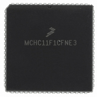
MCHC11F1CFNE3 Freescale Semiconductor, MCHC11F1CFNE3 Datasheet - Page 33

MCHC11F1CFNE3
Manufacturer Part Number
MCHC11F1CFNE3
Description
IC MCU 8BIT 1K RAM 68-PLCC
Manufacturer
Freescale Semiconductor
Series
HC11r
Specifications of MCHC11F1CFNE3
Core Processor
HC11
Core Size
8-Bit
Speed
3MHz
Connectivity
SCI, SPI
Peripherals
POR, WDT
Number Of I /o
30
Program Memory Type
ROMless
Eeprom Size
512 x 8
Ram Size
1K x 8
Voltage - Supply (vcc/vdd)
4.75 V ~ 5.25 V
Data Converters
A/D 8x8b
Oscillator Type
Internal
Operating Temperature
-40°C ~ 85°C
Package / Case
68-PLCC
A/d Inputs
8-Channel, 8-Bit
Eeprom Memory
512 Bytes
Input Output
30
Interface
SCI/SPI
Memory Type
EPROM
Number Of Bits
8
Package Type
68-pin PLCC
Programmable Memory
0 Bytes
Timers
3-16-bit
Voltage, Range
3-5.5 V
Controller Family/series
68HC11
No. Of I/o's
30
Eeprom Memory Size
512Byte
Ram Memory Size
1KB
Cpu Speed
3MHz
No. Of Timers
1
Embedded Interface Type
SCI, SPI
Rohs Compliant
Yes
Processor Series
HC11F
Core
HC11
Data Bus Width
8 bit
Program Memory Size
512 B
Data Ram Size
1 KB
Interface Type
SCI, SPI
Maximum Clock Frequency
3 MHz
Number Of Timers
1
Maximum Operating Temperature
+ 85 C
Mounting Style
SMD/SMT
Minimum Operating Temperature
- 40 C
On-chip Adc
8 bit, 8 Channel
Lead Free Status / RoHS Status
Lead free / RoHS Compliant
Program Memory Size
-
Lead Free Status / Rohs Status
RoHS Compliant part
Available stocks
Company
Part Number
Manufacturer
Quantity
Price
Company:
Part Number:
MCHC11F1CFNE3
Manufacturer:
FREESCALE
Quantity:
5 530
Company:
Part Number:
MCHC11F1CFNE3
Manufacturer:
FREESCALE
Quantity:
5 530
Company:
Part Number:
MCHC11F1CFNE3
Manufacturer:
Freescale Semiconductor
Quantity:
10 000
Company:
Part Number:
MCHC11F1CFNE3R
Manufacturer:
Freescale Semiconductor
Quantity:
10 000
7 Parallel Input/Output
7.1 Port A
7.2 Port B
7.3 Port C
7.4 Port D
7.5 Port E
7.6 Port F
MC68HC11F1/FC0
MC68HC11FTS/D
On the MC68HC11F1, either 54 or 51 pins are available for general-purpose I/O, depending on the
package. These pins are arranged into ports A, B, C, D, E, F, and G. On the MC68HC11FC0, either 52
or 49 pins are available, depending on the package.
I/O functions on some ports (B, C, F, and G) are affected by the mode of operation selected. In the sin-
gle-chip and bootstrap modes, they are configured as parallel I/O data ports. In expanded and test
modes, they are configured as follows:
In addition, in expanded and test modes the R/W signal is configured as data bus direction control. The
remaining ports (A, D, and E) are unaffected by mode changes.
Port A is an eight-bit general-purpose I/O port (PA[7:0]) with a data register (PORTA) and a data direc-
tion register (DDRA). Port A pins are available for shared use among the main timer, pulse accumulator,
and general I/O functions, regardless of mode. Four pins can be used for timer output compare func-
tions (OC), three for input capture (IC), and one as either a fourth IC or a fifth OC.
Port B is an eight-bit general-purpose output-only port in single-chip modes. In expanded modes, port
B pins act as high-order address lines ADDR[15:8], and accesses to PORTB (the port B data register)
are mapped externally.
Port C is an eight-bit general-purpose I/O port with a data register (PORTC) and a data direction register
(DDRC). In single-chip modes, port C pins are general-purpose I/O pins PC[7:0]. Port C can be config-
ured for wired-OR operation in single-chip modes by setting the CWOM bit in the OPT2 register. In ex-
panded modes, port C is the data bus DATA[7:0], and accesses to PORTC (the port C data register)
are mapped externally.
Port D is a six-bit general-purpose I/O port with a data register (PORTD) and a data direction register
(DDRD). In all modes, the six port D lines (PD[5:0]) can be used for general-purpose I/O or for the serial
communications interface (SCI) or serial peripheral interface (SPI) subsystems. Port D can also be con-
figured for wired-OR operation.
Port E is an eight-bit input-only port that is also used (on the MC68HC11F1 only) as the analog input
port for the analog-to-digital converter. Port E pins that are not used for the A/D system can be used as
general-purpose inputs. However, PORTE should not be read during the sample portion of an A/D con-
version sequence.
Port F is an eight-bit output-only port. In single-chip mode, port F pins are general-purpose output pins
PF[7:0]. In expanded mode, port F pins act as low-order address outputs ADDR[7:0].
• Ports B and F are configured as the address bus.
• Port C is configured as the data bus.
• Port G bit 7 is configured as the optional program chip select CSPROG.
PE7 and PE0 are not available on the 80-pin MC68HC11FC0. PE7, PE4, and PE0
are not available on the 64-pin MC68HC11FC0.
Freescale Semiconductor, Inc.
For More Information On This Product,
Go to: www.freescale.com
NOTE
33


