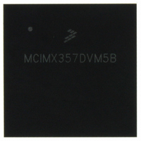
MCIMX357DVM5B Freescale Semiconductor, MCIMX357DVM5B Datasheet - Page 113

MCIMX357DVM5B
Manufacturer Part Number
MCIMX357DVM5B
Description
PROCESSOR MULTIMEDIA 400PBGA
Manufacturer
Freescale Semiconductor
Series
i.MX35r
Datasheet
1.MCIMX35WPDKJ.pdf
(148 pages)
Specifications of MCIMX357DVM5B
Core Processor
ARM11
Core Size
32-Bit
Speed
532MHz
Connectivity
1-Wire, CAN, EBI/EMI, Ethernet, I²C, MMC, SPI, SSI, UART/USART, USB OTG
Peripherals
DMA, I²S, LCD, POR, PWM, WDT
Number Of I /o
96
Program Memory Type
ROMless
Ram Size
128K x 8
Voltage - Supply (vcc/vdd)
1.33 V ~ 1.47 V
Oscillator Type
External
Operating Temperature
-20°C ~ 70°C
Package / Case
400-BGA
Operating Temperature (min)
-20C
Operating Temperature (max)
70C
Operating Temperature Classification
Commercial
Mounting
Surface Mount
Embedded Interface Type
CAN, I2C, SPI, UART, USB
Digital Ic Case Style
BGA
No. Of Pins
400
Operating Temperature Range
-20°C To +70°C
Processor Type
I.MX35
Lead Free Status / RoHS Status
Lead free / RoHS Compliant
Eeprom Size
-
Program Memory Size
-
Data Converters
-
Lead Free Status / Rohs Status
Compliant
Available stocks
Company
Part Number
Manufacturer
Quantity
Price
Company:
Part Number:
MCIMX357DVM5B
Manufacturer:
Freescale Semiconductor
Quantity:
10 000
Part Number:
MCIMX357DVM5B
Manufacturer:
FREESCALE
Quantity:
20 000
Company:
Part Number:
MCIMX357DVM5BR2
Manufacturer:
Freescale Semiconductor
Quantity:
10 000
4.9.22
This section describes electrical characteristics of the SSI.
Freescale Semiconductor
(Output)
STCLK
(Input)
SRCK
SSI Electrical Specifications
•
•
•
•
i.MX35 Applications Processors for Industrial and Consumer Products, Rev. 9
All of the timing for the SSI is given for a non-inverted serial clock
polarity (TSCKP/RSCKP = 0) and a non-inverted frame sync
(TFSI/RFSI = 0). If the polarity of the clock and/or the frame sync have
been inverted, all the timing remains valid by inverting the clock signal
STCK/SRCK and/or the frame sync STFS/SRFS shown in the tables
and in the figures.
All timing is on AUDMUX signals when SSI is being used for data
transfer.
“Tx” and “Rx” refer to the transmit and receive sections of the SSI,
respectively.
For internal frame sync operations using the external clock, the FS
timing will be the same as that of Tx Data (for example, during AC97
mode of operation).
Figure 92. STCLK Timing
Figure 91. SRCK Timing
stclkpl
srckpl
V
V
M
M
NOTE
stclkp
srckp
stclkph
srckph
V
V
M
M
113


