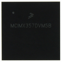
MCIMX357DVM5B Freescale Semiconductor, MCIMX357DVM5B Datasheet - Page 45

MCIMX357DVM5B
Manufacturer Part Number
MCIMX357DVM5B
Description
PROCESSOR MULTIMEDIA 400PBGA
Manufacturer
Freescale Semiconductor
Series
i.MX35r
Datasheet
1.MCIMX35WPDKJ.pdf
(148 pages)
Specifications of MCIMX357DVM5B
Core Processor
ARM11
Core Size
32-Bit
Speed
532MHz
Connectivity
1-Wire, CAN, EBI/EMI, Ethernet, I²C, MMC, SPI, SSI, UART/USART, USB OTG
Peripherals
DMA, I²S, LCD, POR, PWM, WDT
Number Of I /o
96
Program Memory Type
ROMless
Ram Size
128K x 8
Voltage - Supply (vcc/vdd)
1.33 V ~ 1.47 V
Oscillator Type
External
Operating Temperature
-20°C ~ 70°C
Package / Case
400-BGA
Operating Temperature (min)
-20C
Operating Temperature (max)
70C
Operating Temperature Classification
Commercial
Mounting
Surface Mount
Embedded Interface Type
CAN, I2C, SPI, UART, USB
Digital Ic Case Style
BGA
No. Of Pins
400
Operating Temperature Range
-20°C To +70°C
Processor Type
I.MX35
Lead Free Status / RoHS Status
Lead free / RoHS Compliant
Eeprom Size
-
Program Memory Size
-
Data Converters
-
Lead Free Status / Rohs Status
Compliant
Available stocks
Company
Part Number
Manufacturer
Quantity
Price
Company:
Part Number:
MCIMX357DVM5B
Manufacturer:
Freescale Semiconductor
Quantity:
10 000
Part Number:
MCIMX357DVM5B
Manufacturer:
FREESCALE
Quantity:
20 000
Company:
Part Number:
MCIMX357DVM5BR2
Manufacturer:
Freescale Semiconductor
Quantity:
10 000
4.9.5.3
Figure 27
mobile DDR or SDR SDRAM.
Freescale Semiconductor
SD1
SD2
SD3
SD4
SD5
SD6
ID
SDCLK
SDCLK
ADDR
SDRAM clock high-level width
SDRAM clock low-level width
SDRAM clock cycle time
CS, RAS, CAS, WE, DQM, CKE setup time
CS, RAS, CAS, WE, DQM, CKE hold time
Address setup time
through
DQM
RAS
CAS
WE
DQ
CS
ESDCTL Electrical Specifications
SD4
SD6
SD4
i.MX35 Applications Processors for Industrial and Consumer Products, Rev. 9
Figure 36
ROW/BA
Table 33. DDR/SDR SDRAM Read Cycle Timing Parameters
depict the timings pertaining to the ESDCTL module, which interfaces with
SD5
Figure 27. SDRAM Read Cycle Timing Diagram
SD5
Table 33
SD7
SD10
Parameter
SD4
COL/BA
SD4
SD4
through
SD5
SD5
SD5
Table 42
SD8
Note: CKE is high during the read/write cycle.
list the timing parameters.
Data
SD1
SD9
SD3
SD2
Symbol
tCMH
tCMS
tCH
tCK
tAS
tCL
Min.
3.4
3.4
7.0
2.0
1.8
2.0
Max.
4.1
4.1
—
—
—
—
Unit
ns
ns
ns
ns
ns
ns
45


