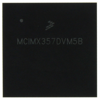
MCIMX357DVM5B Freescale Semiconductor, MCIMX357DVM5B Datasheet - Page 6

MCIMX357DVM5B
Manufacturer Part Number
MCIMX357DVM5B
Description
PROCESSOR MULTIMEDIA 400PBGA
Manufacturer
Freescale Semiconductor
Series
i.MX35r
Datasheet
1.MCIMX35WPDKJ.pdf
(148 pages)
Specifications of MCIMX357DVM5B
Core Processor
ARM11
Core Size
32-Bit
Speed
532MHz
Connectivity
1-Wire, CAN, EBI/EMI, Ethernet, I²C, MMC, SPI, SSI, UART/USART, USB OTG
Peripherals
DMA, I²S, LCD, POR, PWM, WDT
Number Of I /o
96
Program Memory Type
ROMless
Ram Size
128K x 8
Voltage - Supply (vcc/vdd)
1.33 V ~ 1.47 V
Oscillator Type
External
Operating Temperature
-20°C ~ 70°C
Package / Case
400-BGA
Operating Temperature (min)
-20C
Operating Temperature (max)
70C
Operating Temperature Classification
Commercial
Mounting
Surface Mount
Embedded Interface Type
CAN, I2C, SPI, UART, USB
Digital Ic Case Style
BGA
No. Of Pins
400
Operating Temperature Range
-20°C To +70°C
Processor Type
I.MX35
Lead Free Status / RoHS Status
Lead free / RoHS Compliant
Eeprom Size
-
Program Memory Size
-
Data Converters
-
Lead Free Status / Rohs Status
Compliant
Available stocks
Company
Part Number
Manufacturer
Quantity
Price
Company:
Part Number:
MCIMX357DVM5B
Manufacturer:
Freescale Semiconductor
Quantity:
10 000
Part Number:
MCIMX357DVM5B
Manufacturer:
FREESCALE
Quantity:
20 000
Company:
Part Number:
MCIMX357DVM5BR2
Manufacturer:
Freescale Semiconductor
Quantity:
10 000
The i.MX35 core is intended to operate at a maximum frequency of 532 MHz to support the required
multimedia use cases. Furthermore, an image processing unit (IPU) is integrated into the AP domain to
offload the ARM11 core from performing functions such as color space conversion, image rotation and
scaling, graphics overlay, and pre- and post-processing.
The functionality of AP Domain peripherals includes the user interface; the connectivity, display, security,
and memory interfaces; and 128 Kbytes of multipurpose SRAM.
2.2
The shared domain is composed of the shared peripherals, a smart DMA engine (SDMA) and a number of
miscellaneous modules. For maximum flexibility, some peripherals are directly accessible by the SDMA
engine.
The i.MX35 has a hierarchical memory architecture including L1 caches and a unified L2 cache. This
reduces the bandwidth demands for the external bus and external memory. The external memory
subsystem supports a flexible external memory system, including support for SDRAM (SDR, DDR2 and
mobile DDR) and NAND Flash.
2.3
To address the continuing need to reduce power consumption, the following techniques are incorporated
in the i.MX35:
The insertion of gating into the clock paths allows unused portions of the chip to be disabled. Because
static CMOS logic consumes only leakage power, significant power savings can be realized.
“Well biasing” is applying a voltage that is greater than V
to the pwells. The effect of applying this well back bias voltage reduces the subthreshold channel leakage.
For the 90-nm digital process, it is estimated that the subthreshold leakage is reduced by a factor of ten
over the nominal leakage. Additionally, the supply voltage for internal logic can be reduced from 1.4 V to
1.22 V.
2.4
The CPU of the i.MX35 is the ARM1136JF-S core, based on the ARM v6 architecture. This core supports
the ARM Thumb
byte codes) and a range of SIMD DSP instructions that operate on 16-bit or 8-bit data values in 32-bit
registers.
The ARM1136JF-S processor core features are as follows:
6
•
•
•
•
•
•
Clock gating
Power gating
Power-optimized synthesis
Well biasing
Integer unit with integral EmbeddedICE
Eight-stage pipeline
Shared Domain Overview
Advanced Power Management Overview
ARM11 Microprocessor Core
®
i.MX35 Applications Processors for Industrial and Consumer Products, Rev. 9
instruction sets, features Jazelle
™
logic
®
technology (which enables direct execution of Java
DD
to the nwells, and one that is lower than V
Freescale Semiconductor
SS


