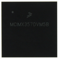
MCIMX357DVM5B Freescale Semiconductor, MCIMX357DVM5B Datasheet - Page 27

MCIMX357DVM5B
Manufacturer Part Number
MCIMX357DVM5B
Description
PROCESSOR MULTIMEDIA 400PBGA
Manufacturer
Freescale Semiconductor
Series
i.MX35r
Datasheet
1.MCIMX35WPDKJ.pdf
(148 pages)
Specifications of MCIMX357DVM5B
Core Processor
ARM11
Core Size
32-Bit
Speed
532MHz
Connectivity
1-Wire, CAN, EBI/EMI, Ethernet, I²C, MMC, SPI, SSI, UART/USART, USB OTG
Peripherals
DMA, I²S, LCD, POR, PWM, WDT
Number Of I /o
96
Program Memory Type
ROMless
Ram Size
128K x 8
Voltage - Supply (vcc/vdd)
1.33 V ~ 1.47 V
Oscillator Type
External
Operating Temperature
-20°C ~ 70°C
Package / Case
400-BGA
Operating Temperature (min)
-20C
Operating Temperature (max)
70C
Operating Temperature Classification
Commercial
Mounting
Surface Mount
Embedded Interface Type
CAN, I2C, SPI, UART, USB
Digital Ic Case Style
BGA
No. Of Pins
400
Operating Temperature Range
-20°C To +70°C
Processor Type
I.MX35
Lead Free Status / RoHS Status
Lead free / RoHS Compliant
Eeprom Size
-
Program Memory Size
-
Data Converters
-
Lead Free Status / Rohs Status
Compliant
Available stocks
Company
Part Number
Manufacturer
Quantity
Price
Company:
Part Number:
MCIMX357DVM5B
Manufacturer:
Freescale Semiconductor
Quantity:
10 000
Part Number:
MCIMX357DVM5B
Manufacturer:
FREESCALE
Quantity:
20 000
Company:
Part Number:
MCIMX357DVM5BR2
Manufacturer:
Freescale Semiconductor
Quantity:
10 000
1
2
4.8.2
Freescale Semiconductor
AC input logic high
AC input logic low
AC differential cross point voltage for output
Duty cycle
Clock frequency
Output pin slew rate
Output pin di/dt
Output pin slew rate (max. drive)
Output pin slew rate (high drive)
Output pin slew rate (standard drive)
Output pin di/dt (max. drive)
Output pin di/dt (high drive)
Output pin di/dt (standard
drive)
The Jedec SSTL_18 specification (JESD8-15a) for an SSTL interface for class II operation supersedes any specification in this
document.
The typical value of Vox(ac) is expected to be about 0.5 × NVCC and Vox(ac) is expected to track variation in NVCC. Vox(ac)
indicates the voltage at which the differential output signal must cross. Cload = 25 pF.
AC Electrical Characteristics for DDR Pins (DDR2, Mobile DDR, and
SDRAM Modes)
Parameter
Table 20. AC Electrical Characteristics of GPIO Pins in Fast Slew Rate Mode
Table 21. AC Electrical Characteristics of DDR Type IO Pins in DDR2 Mode
i.MX35 Applications Processors for Industrial and Consumer Products, Rev. 9
Parameter
Parameter
1
Table 22. AC Requirements of DDR2 Pins
[NVCC = 2.25 V–2.75 V] (continued)
2
Symbol
Fduty
tps
tdit
f
Symbol
Test Condition
tps
tps
tps
tdit
tdit
tdit
25 pF
50 pF
25 pF
50 pF
Symbol
VIH(ac)
Vox(ac)
VIL(ac)
—
—
Condition
25 pF
40 pF
50 pF
25 pF
40 pF
50 pF
25 pF
40 pF
50 pF
25 pF
50 pF
25 pF
50 pF
25 pF
50 pF
Test
NVCC ÷ 2 – 0.125
NVCC ÷ 2 + 0.25
0.86/0.98
Rise/Fall
0.46/054
0.84/1.10
0.68/0.83
0.58/0.72
0.69/0.96
0.55/0.69
0.40/0.59
0.24/0.36
0.37/0.47
0.13/0.21
Rise/Fall
Min.
45
65
70
—
Min.
Min.
–0.3
46
49
33
35
28
29
1.45/1.80
1.14/1.34
0.86/1.10
1.18/1.50
0.92/1.10
0.67/0.95
0.80/1.00
0.62/0.76
0.45/0.65
0.72/0.81
1.35/1.5
Typ.
124
131
Typ.
89
94
75
79
133
157
167
50
NVCC ÷ 2 + 0.125
NVCC ÷ 2 – 0.25
Rise/Fall
2.40/2.80
1.88/2.06
1.40/1.70
1.90/2.30
1.49/1.67
1.10/1.30
1.30/1.60
1.00/1.14
0.70/0.95
NVCC + 0.3
Max.
310
324
290
304
188
198
2.15/2.19
1.12/1.16
Rise/Fall
Max.
Max.
373
396
55
—
mA/ns
mA/ns
mA/ns
Units Notes
V/ns
V/ns
V/ns
mA/ns
Units
MHz
V/ns
V
V
V
%
Units
2
3
27


