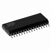
CLRC63201T/0FE,112 NXP Semiconductors, CLRC63201T/0FE,112 Datasheet - Page 67

CLRC63201T/0FE,112
Manufacturer Part Number
CLRC63201T/0FE,112
Description
IC I.CODE HS READER 32-SOIC
Manufacturer
NXP Semiconductors
Series
I-Coder
Specifications of CLRC63201T/0FE,112
Rf Type
Read Only
Frequency
13.56MHz
Features
ISO14443-A, ISO14443-B, ISO15693, ISO18000-3
Package / Case
32-SOIC (0.300", 7.50mm Width)
Product
RFID Readers
Operating Temperature Range
- 25 C to + 85 C
Lead Free Status / RoHS Status
Lead free / RoHS Compliant
Lead Free Status / RoHS Status
Lead free / RoHS Compliant, Lead free / RoHS Compliant
Other names
568-2199-5
935269690112
CLRC632
CLRC63201TD
935269690112
CLRC632
CLRC63201TD
Available stocks
Company
Part Number
Manufacturer
Quantity
Price
Company:
Part Number:
CLRC63201T/0FE,112
Manufacturer:
IR
Quantity:
3 400
Part Number:
CLRC63201T/0FE,112
Manufacturer:
NXP/恩智浦
Quantity:
20 000
NXP Semiconductors
CLRC632_35
Product data sheet
PUBLIC
10.5.4.7 RxControl2 register
10.5.4.8 ClockQControl register
Controls decoder behavior and defines the input source for the receiver.
Table 95.
Table 96.
[1]
Controls clock generation for the 90 phase-shifted Q-clock.
Table 97.
Table 98.
Bit
Symbol
Access
Bit
7
6
5 to 2
1 to 0
Bit
Symbol
Access
Bit
7
6
5
4 to 0
I-clock and Q-clock are 90 phase-shifted from each other.
Symbol
RcvClkSelI
RxAutoPD
0000
DecoderSource[1:0]
Symbol
ClkQ180Deg
ClkQCalib
0
ClkQDelay[4:0]
RxControl2 register (address: 1Eh) reset value: 0100 0001b, 41h bit allocation
RxControl2 register bit descriptions
ClockQControl register (address: 1Fh) reset value: 000x xxxxb, xxh bit allocation
ClockQControl register bit descriptions
RcvClkSelI
ClkQ180Deg ClkQCalib
R/W
7
R
7
Rev. 3.5 — 10 November 2009
RxAutoPD
R/W
Value
1
0
0
1
-
-
Multiple protocol contactless reader IC (MIFARE/I-CODE1)
6
R/W
Value Description
1
0
1
0
-
00
01
10
11
073935
6
Description
Q-clock is phase-shifted more than 180 compared to the
I-clock
Q-clock is phase-shifted less than 180 compared to the
I-clock
Q-clock is automatically calibrated after the reset phase and
after data reception from the card
no calibration is performed automatically
this value must not be changed
this register shows the number of delay elements used to
generate a 90 phase-shift of the I-clock to obtain the
Q-clock. It can be written directly by the microprocessor or
by the automatic calibration cycle.
I-clock is used as the receiver clock
Q-clock is used as the receiver clock
receiver circuit is automatically switched on before
receiving and switched off afterwards. This can be used to
reduce current consumption.
receiver is always activated
these values must not be changed
selects the source for the decoder input
5
LOW
internal demodulator
a subcarrier modulated Manchester encoded signal on
pin MFIN
a baseband Manchester encoded signal on pin MFIN
R/W
5
0
4
4
0000
R/W
3
3
ClkQDelay[4:0]
2
2
D
[1]
CLRC632
[1]
DecoderSource[1:0]
© NXP B.V. 2009. All rights reserved.
1
1
R/W
67 of 126
0
0


