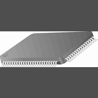
CR16MCS9VJE8 National Semiconductor, CR16MCS9VJE8 Datasheet - Page 29

CR16MCS9VJE8
Manufacturer Part Number
CR16MCS9VJE8
Description
16-Bit Microcontroller IC
Manufacturer
National Semiconductor
Datasheet
1.CR16MCS9VJE8.pdf
(156 pages)
Specifications of CR16MCS9VJE8
Controller Family/series
CR16X
Core Size
16 Bit
Program Memory Size
64K X 8 Flash
Digital Ic Case Style
PQFP
No. Of Pins
80
Mounting Type
Surface Mount
Clock Frequency
25MHz
Lead Free Status / RoHS Status
Contains lead / RoHS non-compliant
Available stocks
Company
Part Number
Manufacturer
Quantity
Price
Company:
Part Number:
CR16MCS9VJE8
Manufacturer:
ON
Quantity:
8 917
Company:
Part Number:
CR16MCS9VJE8-CBB
Manufacturer:
ON
Quantity:
846
Company:
Part Number:
CR16MCS9VJE8-CBC
Manufacturer:
ON
Quantity:
109
Company:
Part Number:
CR16MCS9VJE8-CBD
Manufacturer:
ON
Quantity:
17
Company:
Part Number:
CR16MCS9VJE8-CBE
Manufacturer:
ON
Quantity:
1 950
however, the even numbered bytes of the high endurance
flash EEPROM data memory (F000 to F07E) and the ISP
flash EEPROM program memory (E000 to E5FE) can be
erased.
Read/write is overridden through PADX.
E5FC Byte
Upon reset of the chip, E5FC is read into the FLCTRL2 reg-
ister. The byte at E5FC is written in the ISP or test environ-
ments, or in the IRE environment through a byte-write
instruction when the write instruction is anywhere within the
user boot ROM area except for the last two words. When the
user boot ROM area has been disabled by having a value of
7F
IRE environment. Note that when this word is erased for re-
programming, the other words in the same page must first be
saved, and then re-programmed also. The E5FC register for-
mat is shown below:
This byte contains the lowest 8 bits of the CODEAREA field.
When appended to the left with the lowest 2 bits in the ad-
dress E5FE, it forms the complete CODEAREA field, which
provides write protection to all or part of the program memo-
ry, see Figure3. When write security is not enabled and
CODEAREA does not contain the value 3FF
memory range from (CODEAREA 128) to 1FFFF is consid-
ered as protected user code area and cannot be written. The
minimum protected memory range is therefore 256 bytes
when CODEAREA contains the value 3FE. Note that the
C000-FFFF memory range is not considered as program
memory and is not protected by CODEAREA.
When CODEAREA contains the value 3FF
tion is disabled. When the user code area overlaps into the
user boot ROM area, the overlap area is governed by a more
restrictive write protection feature, which is the user boot
ROM area. When write security has been enabled, the entire
program memory area is already write protected in all envi-
ronments.
Note that when a new value is written into CODEAREA, write
protection controlled by CODEAREA is updated after the
next device reset.
7
16
Figure 3. Memory Protection through CODEAREA
1FFFFh
10000h
C000h
0000h
in BOOTAREA, this word cannot be programmed in the
Address Map
CR16MHR6
non-code area, not
protected
protected
code area
protected
code area
CODEAREA[7:0]
user
user
CODEAREA 128
16
16
, write protec-
, the program
0
29
E5FD Byte
Upon the reset of the chip, the byte located at the E5FD ad-
dress is read into the FLCTRL1 register. This byte can only
be written in the ISP or test environments but not in the IRE
environment. If this byte is erased for re-programming, the
user must first save the other bytes in the same page, and
then re-program those bytes. The format of the E5FD byte is
shown below:
BOOTAREA provides write protection to part of the program
memory, see Figure4. When the write security feature is not
enabled and BOOTAREA does not contain the value 7F
then the program memory range from 0 to (BOOTAR-
EA*128)+127 is considered as user boot ROM area and can-
not be written to. The maximum protected memory range is
therefore 16K-127 bytes when BOOTAREA contains the val-
ue 7E
When BOOTAREA contains the value 7F
is disabled. When write security has been enabled, the entire
program memory area is already write protected in all envi-
ronments.
Note that when a new value is written into BOOTAREA, write
protection controlled by BOOTAREA is updated after the
next device reset.
9.4.6
The ISP flash EEPROM program memory test mode allows
direct access to the flash memory from the device pins, and
bypasses the CR16B core. This test mode also accesses the
flash memory cells that are not used in data memory (three
out of four bytes in each page).
9.4.7
The FLCTRL1 register is a read-only byte-wide register. The
value of this register is loaded from memory address E5FD
when the chip comes out of reset. The BOOTAREA field de-
fines a user boot ROM area to be write protected. The Flash
EEPROM Program Memory Control Register 1 format is
shown below:
1FFFFh
0000h
Figure 4.
3F80h
Reserved
Reserved
16
.
Test Mode
Flash Program Memory Control Register 1
(FLCTRL1)
7
CR16MHR6
7
Address Map
protected user boot
area
Memory Protection through BOOTAREA
6
6
BOOTAREA
BOOTAREA
boot area maximum limit
(BOOTAREA 128)+127
16
www.national.com
, write protection
16
0
16
0
,


