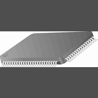
CR16MCS9VJE8 National Semiconductor, CR16MCS9VJE8 Datasheet - Page 30

CR16MCS9VJE8
Manufacturer Part Number
CR16MCS9VJE8
Description
16-Bit Microcontroller IC
Manufacturer
National Semiconductor
Datasheet
1.CR16MCS9VJE8.pdf
(156 pages)
Specifications of CR16MCS9VJE8
Controller Family/series
CR16X
Core Size
16 Bit
Program Memory Size
64K X 8 Flash
Digital Ic Case Style
PQFP
No. Of Pins
80
Mounting Type
Surface Mount
Clock Frequency
25MHz
Lead Free Status / RoHS Status
Contains lead / RoHS non-compliant
Available stocks
Company
Part Number
Manufacturer
Quantity
Price
Company:
Part Number:
CR16MCS9VJE8
Manufacturer:
ON
Quantity:
8 917
Company:
Part Number:
CR16MCS9VJE8-CBB
Manufacturer:
ON
Quantity:
846
Company:
Part Number:
CR16MCS9VJE8-CBC
Manufacturer:
ON
Quantity:
109
Company:
Part Number:
CR16MCS9VJE8-CBD
Manufacturer:
ON
Quantity:
17
Company:
Part Number:
CR16MCS9VJE8-CBE
Manufacturer:
ON
Quantity:
1 950
www.national.com
When BOOTAREA has any value other than 7F
memory at 0 to (BOOTAREA 128)+15 is considered as user
boot ROM area and is write protected. When it has a value of
7F
tected
9.4.8
The FLCTRL2 register is a read-only word-wide register. The
value of this register is loaded from memory addresses
E5FC
the device starts execution, the EMPTY bit indicates whether
the flash EEPROM program memory is empty of not, and se-
lects the chip to be in IRE or ISP environment if the external
environment pins are all high. The CODEAREA field defines
a user code area to be write protected. The Flash EEPROM
Program Memory Control Register 2 format is shown below:
EMPTY
CODEAREA When it has any value other than 3FF
9.4.9
The FLSEC register is a read-only byte-wide register. When
the chip comes out of reset, the value of this register is load-
ed from memory address E5FF
FROMWR field control the read and write security of the flash
EEPROM program memory respectively. The Flash EE-
PROM Program Memory Security register format is shown
below:
0000, 0001, 0010, 0100, 1000: Security feature enabled
0011, 0101, 011x, 1001, 101x, 11xx: Security feature disabled
FROMRD
FROMWR
7
15
16
, then there is no user boot ROM area to be write pro-
1 6
EMPTY
and E5FE
Flash Program Memory Control Register 2
(FLCTRL2)
Flash Program Memory Security Register
(FLSEC)
FROMWR
When the bits are either 011
111
pins are all high, the device will come out of re-
set in ISP environment instead of IRE environ-
ment.
the memory (CODEAREA 128) to 1FFFF
considered as user code area and is write pro-
tected. When it has a value of 3FF
is no code protection area to be write protect-
ed.
When read security feature is enabled, the
flash EEPROM program memory can only be
read in IRE environment, but will return 0000
in other environments; also, erase to odd num-
bered bytes from address E5F9
and mass erase to ISP and flash EEPROM
data memory array are ignored unless PADX is
activated (see security override below).
Unless PADX is activated (see override below),
when write security feature is enabled, all fur-
ther writes and erases to flash EEPROM pro-
gram memory, erase to odd numbered bytes
from address E5F9
erase to ISP and flash EEPROM data memory
array are ignored.
2
13 12
1 6
, and if the device’s environment select
when the chip comes out of reset. When
Reserved
4 3
16
16
10 9
. The FROMRD and
to E5FF
FROMRD
2
, 101
CODEAREA
16
16
1 6
, and mass
1 6
, then there
2
to E5FF
, then the
, 110
16
, then
2
16
, or
1 6
1 6
0
is
0
30
9.4.10
The In-System-Programming Memory Write Key (ISPKEY)
register is a byte-wide, write-only register. It contains the en-
able key to enable writes to ISP flash EEPROM program
memory. A value of 6A
mediately preceding every write to the ISP flash EEPROM
program memory for the flash write operation to proceed,
otherwise any other write operation will clear the key (the
only exception is that the subsequent write is another write to
this key register with the proper key, in which case the key is
still set). A read always returns FF
reset, the write enable status that is generated as a result of
a write to this key register is cleared. The ISP Memory Write
Key register format is shown below:
ISPKYVAL is the ISP Flash Program Memory Write Enable
Key Value.
7
ISP Memory Write Key Register (ISPKEY)
16
ISPKYVAL
must be written to this register im-
1 6
. Engineering note: on
0


