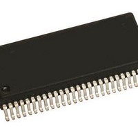
MM908E625ACDWB Freescale Semiconductor, MM908E625ACDWB Datasheet - Page 21

MM908E625ACDWB
Manufacturer Part Number
MM908E625ACDWB
Description
IC QUAD HALF BRDG MCU/LIN 54SOIC
Manufacturer
Freescale Semiconductor
Datasheets
1.MM908E625.pdf
(48 pages)
2.MM908E625ACDWB.pdf
(48 pages)
3.MM908E625ACDWB.pdf
(48 pages)
4.MM908E625ACDWB.pdf
(48 pages)
5.MM908E625ACDWB.pdf
(40 pages)
Specifications of MM908E625ACDWB
Applications
Automotive Mirror Control
Core Processor
HC08
Program Memory Type
FLASH (16 kB)
Controller Series
908E
Ram Size
512 x 8
Interface
SCI, SPI
Number Of I /o
13
Voltage - Supply
8 V ~ 18 V
Operating Temperature
-40°C ~ 85°C
Mounting Type
Surface Mount
Package / Case
54-SOIC (0.300", 7.50mm Width) Exposed Pad
Program Memory Size
16 KB
Number Of Programmable I/os
54
Number Of Timers
16
Operating Supply Voltage
- 18 V to + 28 V
Maximum Operating Temperature
+ 85 C
Mounting Style
SMD/SMT
Minimum Operating Temperature
- 40 C
Lead Free Status / RoHS Status
Contains lead / RoHS non-compliant
Available stocks
Company
Part Number
Manufacturer
Quantity
Price
Company:
Part Number:
MM908E625ACDWB
Manufacturer:
FREESCALE Semiconductor
Quantity:
26
INTERRUPT FLAG REGISTER (IFR
Hall-Effect Sensor Input Pin Flag Bit (HPF)
mode.
RUN Mode
enabled Hall-effect sensor input pin is detected. Clear HPF
by writing a Logic [1] to HPF. Reset clears the HPF bit.
Writing a Logic [0] to HPF has no effect.
STOP Mode
current above the threshold is detected on any enabled Hall-
effect sensor input pin. Clear HPF by writing a Logic [1] to
HPF. Reset clears the HPF bit. Writing a Logic [0] to HPF has
no effect.
data line. Clear LINF by writing a Logic [1] to LINF. Reset
clears the LINF bit. Writing a Logic [0] to LINF has no effect.
High-Temperature Flag Bit (HTF)
Clear HTF by writing a Logic [1] to HTF. If a high-temperature
LIN Flag Bit (LINF)
Analog Integrated Circuit Device Data
Freescale Semiconductor
Reset
Write
Read
Bits
This read/write flag is set depending on RUN/STOP
An interrupt will be generated when a state change on any
• 1 = State change on the hallflags detected
• 0 = No state change on the hallflags detected
An interrupt will be generated when AWDCC is set and a
• 1 = One or more of the selected Hall-effect sensor input
• 0 = None of the selected Hall-effect sensor input pins
This read/write flag is set on the falling edge at the LIN
• 1 = Falling edge on LIN data line has occurred
• 0 = Falling edge on LIN data line has not occurred since
This read/write flag is set on a high-temperature condition.
pins had been pulled HIGH
has been pulled HIGH
last clear
0
0
7
Register Name and Address: IFR - $05
HPF
6
0
LINF
5
0
HTF
4
0
LVF
3
0
LOGIC COMMANDS AND REGISTERS
)
HVF
2
0
OCF
1
0
0
0
0
condition is still present while writing a Logic [1] to HTF, the
writing has no effect. Therefore, a high-temperature interrupt
cannot be lost due to inadvertent clearing of HTF. Reset
clears the HTF bit. Writing a Logic [0] to HTF has no effect.
Low-Voltage Flag Bit (LVF)
LVF by writing a Logic [1] to LVF. If a low-voltage condition is
still present while writing a Logic [1] to LVF, the writing has no
effect. Therefore, a low-voltage interrupt cannot be lost due
to inadvertent clearing of LVF. Reset clears the LVF bit.
Writing a Logic [0] to LVF has no effect.
High-Voltage Flag Bit (HVF)
Clear HVF by writing a Logic [1] to HVF. If high-voltage
condition is still present while writing a Logic [1] to HVF, the
writing has no effect. Therefore, a high-voltage interrupt
cannot be lost due to inadvertent clearing of HVF. Reset
clears the HVF bit. Writing a Logic [0] to HVF has no effect.
Overcurrent Flag Bit (OCF)
Reset clears the OCF bit. To clear this flag, write a Logic [1]
to the appropriate overcurrent flag in the SYSSTAT Register.
See
OCF.
• 1 = High-temperature condition has occurred
• 0 = High-temperature condition has not occurred
This read/write flag is set on a low-voltage condition. Clear
• 1 = Low-voltage condition has occurred
• 0 = Low-voltage condition has not occurred
This read/write flag is set on a high-voltage condition.
• 1 = High-voltage condition has occurred
• 0 = High-voltage condition has not occurred
This read-only flag is set on an overcurrent condition.
• 1 = High-current condition has occurred
• 0 = High-current condition has not occurred
Figure
Figure 10. Principal Implementation for OCF
10,illustrating the three signals triggering the
HVDD_OCF
HS_OCF
HB_OCF
LOGIC COMMANDS AND REGISTERS
FUNCTIONAL DEVICE OPERATION
OCF
908E625
21


