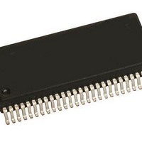
MM908E625ACDWB Freescale Semiconductor, MM908E625ACDWB Datasheet - Page 5

MM908E625ACDWB
Manufacturer Part Number
MM908E625ACDWB
Description
IC QUAD HALF BRDG MCU/LIN 54SOIC
Manufacturer
Freescale Semiconductor
Datasheets
1.MM908E625.pdf
(48 pages)
2.MM908E625ACDWB.pdf
(48 pages)
3.MM908E625ACDWB.pdf
(48 pages)
4.MM908E625ACDWB.pdf
(48 pages)
5.MM908E625ACDWB.pdf
(40 pages)
Specifications of MM908E625ACDWB
Applications
Automotive Mirror Control
Core Processor
HC08
Program Memory Type
FLASH (16 kB)
Controller Series
908E
Ram Size
512 x 8
Interface
SCI, SPI
Number Of I /o
13
Voltage - Supply
8 V ~ 18 V
Operating Temperature
-40°C ~ 85°C
Mounting Type
Surface Mount
Package / Case
54-SOIC (0.300", 7.50mm Width) Exposed Pad
Program Memory Size
16 KB
Number Of Programmable I/os
54
Number Of Timers
16
Operating Supply Voltage
- 18 V to + 28 V
Maximum Operating Temperature
+ 85 C
Mounting Style
SMD/SMT
Minimum Operating Temperature
- 40 C
Lead Free Status / RoHS Status
Contains lead / RoHS non-compliant
Available stocks
Company
Part Number
Manufacturer
Quantity
Price
Company:
Part Number:
MM908E625ACDWB
Manufacturer:
FREESCALE Semiconductor
Quantity:
26
Table 2. Maximum Ratings
permanent damage to the device.
Analog Integrated Circuit Device Data
Freescale Semiconductor
ELECTRICAL RATINGS
THERMAL RATINGS
Notes
Supply Voltage
Input Pin Voltage
Maximum Microcontroller Current per Pin
Maximum Microcontroller V
Maximum Microcontroller V
LIN Supply Voltage
ESD Voltage
Storage Temperature
Ambient Operating Temperature
Operating Case Temperature
Operating Junction Temperature
Peak Package Reflow Temperature During Solder Mounting
All voltages are with respect to ground unless otherwise noted. Exceeding these ratings may cause a malfunction or
1.
2.
3.
4.
5.
6.
7.
Analog Chip Supply Voltage under Normal Operation, Steady State
Analog Chip Supply Voltage under Transient Conditions
Microcontroller Chip Supply Voltage
Analog Chip
Microcontroller Chip
All Pins Except VDD, VSS, PTA0:PTA6, PTC0:PTC1
Pins PTA0:PTA6, PTC0:PTC1
Normal Operation (Steady-State)
Transient Conditions
Human Body Model (HBM)
Machine Model (MM)
Charge Device Model (CDM)
Transient capability for pulses with a time of t < 0.5 sec.
ESD voltage testing is performed in accordance with the Human Body Model (C
ESD voltage testing is performed in accordance with the Machine Model (C
ESD voltage testing is performed in accordance with Charge Device Model, robotic (C
The limiting factor is junction temperature, taking into account the power dissipation, thermal resistance, and heat sinking.
The temperature of analog and MCU die is strongly linked via the package, but can differ in dynamic load conditions, usually because
of higher power dissipation on the analog die. The analog die temperature must not exceed 150°C under these conditions.
Pin soldering temperature is for 10 seconds maximum duration. Not designed for immersion soldering. Exceeding these limits may cause
malfunction or permanent damage to the device.
(1)
(3)
SS
DD
(2)
(5)
Output Current
Input Current
(4)
(6)
Ratings
ELECTRICAL CHARACTERISTICS
MAXIMUM RATINGS
(1)
(7)
V
ZAP
V
BUS(DYNAMIC)
IN
V
V
V
V
T
Symbol
=200 pF, R
SOLDER
ZAP
SUP(
SUP(
IN
I
I
I
BUS(SS)
I
(ANALOG)
V
PIN
PIN
T
MVSS
MVDD
V
T
T
ESD
STG
T
(MCU)
DD
A
C
J
= 100 pF, R
(1)
(2)
SS
PK
ZAP
)
)
=4.0 pF).
ZAP
= 0 Ω)
V
ZAP
SS
ELECTRICAL CHARACTERISTICS
-0.3 to V
= 1500 Ω)
-0.3 to 6.0
-0.3 to 5.5
-40 to 150
-40 to 125
-0.3 to 28
-0.3 to 40
-40 to 85
-40 to 85
-18 to 28
±3000
Value
±150
±500
±25
±15
100
100
245
40
DD
+0.3
MAXIMUM RATINGS
Unit
mA
mA
mA
°C
°C
°C
°C
°C
V
V
V
V
908E625
5


