MM908E625ACDWB Freescale Semiconductor, MM908E625ACDWB Datasheet - Page 46
MM908E625ACDWB
Manufacturer Part Number
MM908E625ACDWB
Description
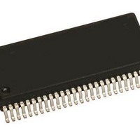
IC QUAD HALF BRDG MCU/LIN 54SOIC
Manufacturer
Freescale Semiconductor
Datasheets
1.MM908E625.pdf
(48 pages)
2.MM908E625ACDWB.pdf
(48 pages)
3.MM908E625ACDWB.pdf
(48 pages)
4.MM908E625ACDWB.pdf
(48 pages)
5.MM908E625ACDWB.pdf
(40 pages)
Specifications of MM908E625ACDWB
Applications
Automotive Mirror Control
Core Processor
HC08
Program Memory Type
FLASH (16 kB)
Controller Series
908E
Ram Size
512 x 8
Interface
SCI, SPI
Number Of I /o
13
Voltage - Supply
8 V ~ 18 V
Operating Temperature
-40°C ~ 85°C
Mounting Type
Surface Mount
Package / Case
54-SOIC (0.300", 7.50mm Width) Exposed Pad
Program Memory Size
16 KB
Number Of Programmable I/os
54
Number Of Timers
16
Operating Supply Voltage
- 18 V to + 28 V
Maximum Operating Temperature
+ 85 C
Mounting Style
SMD/SMT
Minimum Operating Temperature
- 40 C
Lead Free Status / RoHS Status
Contains lead / RoHS non-compliant
Available stocks
Company
Part Number
Manufacturer
Quantity
Price
Company:

Part Number:
MM908E625ACDWB
Manufacturer:
FREESCALE Semiconductor
Quantity:
26


ADDITIONAL DOCUMENTATION
THERMAL ADDENDUM (REV 2.0)
Introduction
technical data sheet. The addendum provides thermal performance information
that may be critical in the design and development of system applications. All
electrical, application and packaging information is provided in the data sheet.
Package and Thermal Considerations
package independently heating with P
temperatures, T
temperature while only heat source 1 is heating with P
reference temperature while heat source 2 is heating with P
R
package to another in a standardized environment. This methodology is not
meant to and will not predict the performance of a package in an application-specific environment. Stated values were obtained
by measurement and simulation according to the standards listed below.
Standards
Table 14. Thermal Performance Comparison
46
908E625
ADDITIONAL DOCUMENTATION
THERMAL ADDENDUM (REV 2.0)
Notes:
θ J21
This thermal addendum ia provided as a supplement to the MM908E625
This MM908E625 is a dual die package. There are two heat sources in the
For m, n = 1, R
For m = 1, n = 2, R
The stated values are solely for a thermal performance comparison of one
Resistance
1.
2.
3.
4.
5.
R
R
R
R
Thermal
θ
θ
θ
θJCmn
JA mn
JB mn
JA mn
and R
Per JEDEC JESD51-2 at natural convection, still air
condition.
2s2p thermal test board per JEDEC JESD51-7and
JESD51-5.
Per JEDEC JESD51-8, with the board temperature on the
center trace near the power outputs.
Single layer thermal test board per JEDEC JESD51-3 and
JESD51-5.
Thermal resistance between the die junction and the
exposed pad, “infinite” heat sink attached to exposed pad.
(5)
(1)(2)
(2)(3)
(1)(4)
θ J22
T
T
J1
, respectively.
J1
J2
θ JA11
and T
m = 1,
1 = Power Chip, 2 = Logic Chip
n = 1
=
9.0
1.0
23
52
θ JA12
is the thermal resistance from Junction 1 to the reference
J2
R
R
, and a thermal resistance matrix with R
θ JA11
θ JA21
is the thermal resistance from Junction 1 to the
m = 1, n = 2
m = 2, n = 1
R
R
θ JA12
θ JA22
6.0
20
47
0
1
and P
.
P
P
2
. This results in two junction
1
2
[°C/W]
m = 2,
n = 2
2.0
24
10
52
1
.
2
. This applies to
θ JA mn
Attachment Per JEDEC JESD51-5Thermal Test Board
Figure 27. Thermal Land Pattern for Direct Thermal
.
10.3 mm x 5.1 mm Exposed Pad
17.9 mm x 7.5 mm Body
54 Terminal SOIC-EP
0.65 mm Pitch
Note For package dimensions, refer to the
908E625 device datasheet.
Analog Integrated Circuit Device Data
EK SUFFIX (Pb-Free)
54-PIN SOICW-EP
98ARL105910
DWB SUFFIX
908E625
SOICW-EP
54-PIN
Freescale Semiconductor
0.2
* All measurements
are in millimeters
Soldermast
openings
Thermal vias
connected to top
buried plane
1.0
0.2
1.0
Related parts for MM908E625ACDWB
Image
Part Number
Description
Manufacturer
Datasheet
Request
R

Part Number:
Description:
Integrated Quad Half H-bridge With Power Supply, Embedded Mcu, And Lin Serial Communication
Manufacturer:
Freescale Semiconductor, Inc
Datasheet:

Part Number:
Description:
KIT EVAL PRELIM MM98E625/26
Manufacturer:
Freescale Semiconductor
Datasheet:
Part Number:
Description:
Manufacturer:
Freescale Semiconductor, Inc
Datasheet:
Part Number:
Description:
Manufacturer:
Freescale Semiconductor, Inc
Datasheet:
Part Number:
Description:
Manufacturer:
Freescale Semiconductor, Inc
Datasheet:
Part Number:
Description:
Manufacturer:
Freescale Semiconductor, Inc
Datasheet:
Part Number:
Description:
Manufacturer:
Freescale Semiconductor, Inc
Datasheet:
Part Number:
Description:
Manufacturer:
Freescale Semiconductor, Inc
Datasheet:
Part Number:
Description:
Manufacturer:
Freescale Semiconductor, Inc
Datasheet:
Part Number:
Description:
Manufacturer:
Freescale Semiconductor, Inc
Datasheet:
Part Number:
Description:
Manufacturer:
Freescale Semiconductor, Inc
Datasheet:
Part Number:
Description:
Manufacturer:
Freescale Semiconductor, Inc
Datasheet:
Part Number:
Description:
Manufacturer:
Freescale Semiconductor, Inc
Datasheet:
Part Number:
Description:
Manufacturer:
Freescale Semiconductor, Inc
Datasheet:
Part Number:
Description:
Manufacturer:
Freescale Semiconductor, Inc
Datasheet: