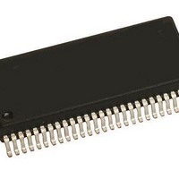
MM908E625ACDWB Freescale Semiconductor, MM908E625ACDWB Datasheet - Page 41

MM908E625ACDWB
Manufacturer Part Number
MM908E625ACDWB
Description
IC QUAD HALF BRDG MCU/LIN 54SOIC
Manufacturer
Freescale Semiconductor
Datasheets
1.MM908E625.pdf
(48 pages)
2.MM908E625ACDWB.pdf
(48 pages)
3.MM908E625ACDWB.pdf
(48 pages)
4.MM908E625ACDWB.pdf
(48 pages)
5.MM908E625ACDWB.pdf
(40 pages)
Specifications of MM908E625ACDWB
Applications
Automotive Mirror Control
Core Processor
HC08
Program Memory Type
FLASH (16 kB)
Controller Series
908E
Ram Size
512 x 8
Interface
SCI, SPI
Number Of I /o
13
Voltage - Supply
8 V ~ 18 V
Operating Temperature
-40°C ~ 85°C
Mounting Type
Surface Mount
Package / Case
54-SOIC (0.300", 7.50mm Width) Exposed Pad
Program Memory Size
16 KB
Number Of Programmable I/os
54
Number Of Timers
16
Operating Supply Voltage
- 18 V to + 28 V
Maximum Operating Temperature
+ 85 C
Mounting Style
SMD/SMT
Minimum Operating Temperature
- 40 C
Lead Free Status / RoHS Status
Contains lead / RoHS non-compliant
Available stocks
Company
Part Number
Manufacturer
Quantity
Price
Company:
Part Number:
MM908E625ACDWB
Manufacturer:
FREESCALE Semiconductor
Quantity:
26
DEVELOPMENT SUPPORT
embedded typically all the development tools available for
the MCU also apply for this device, however due to the fact
of the additional analog die circuitry and the nominal +12V
supply voltage some additional items have to be considered:
development support see the MC68HC908EY16 datasheet -
section development support.
Vsup (12V) instead as descibted in
Analog Integrated Circuit Device Data
Freescale Semiconductor
RS232
2
3
5
DB-9
As the 908E625 has the MC68HC908EY16 MCU
• nominal 12V rather than 5V or 3V supply
• high voltage V
For a detailed information on the MCU related
Of course its also possible to supply the whole system with
but IRQ_A pin
1µF
1µF
+
+
1
3
4
5
7
8
C1+
C1-
C2+
C2-
T2
R2
OUT
IN
TST
MAX232
might be applied not only to IRQ pin,
R2
GND
V
T2
OUT
V+
V-
CC
IN
16
15
2
6
10
9
+5V
2
74HC125
Figure
+
Figure 23. Normal Monitor Mode Circuit (MCU only)
+
1
1µF
1µF
3
+
24,
1µF
6
74HC125
TYPICAL APPLICATIONS
page
4
5
42.
+5V
10k
V
TST
9.8304MHz CLOCK
the manufacturing process - first on chip level, before the IC
is soldered onto a pcb board and second after the IC is
soldered onto the pcb board.
Chip level programming
with +5V (see
with VSUP, in this setup all the analog pin should be left open
(e.g. VSUP[1:3]) and interconnections between MCU and
analog die have to be separated (e.g.
datasheet - section development support.
PCB level programming
possible to seperately power the MCU with +5V, the whole
The programming is principially possible at two stages in
On Chip level the easiest way is to only power the MCU
This mode is well descripted in the MC68HC908EY16
If the IC is soldered onto the pcb board its typically not
DATA
CLK
Figure
VSUP[1:3]
GND[1:2]
RST
RST_A
IRQ
IRQ_A
PTC4/OSC1
PTA0/KBD0
FACTORY TRIMMING AND CALIBRATION
23) and not to provide the analog chip
MM908E625
PTA1/KBD1
PTB4/AD4
PTB3/AD3
TYPICAL APPLICATIONS
VREFH
VREFL
VDDA
EVDD
VSSA
EVSS
VDD
IRQ
VSS
-
100nF
IRQ_A
10k
10k
10k
+5V
).
908E625
+5V
4.7µF
41


