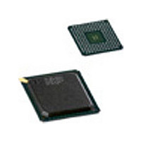
PNX1302EH NXP Semiconductors, PNX1302EH Datasheet - Page 190

PNX1302EH
Manufacturer Part Number
PNX1302EH
Description
Manufacturer
NXP Semiconductors
Datasheet
1.PNX1302EH.pdf
(548 pages)
Specifications of PNX1302EH
Lead Free Status / RoHS Status
Not Compliant
Available stocks
Company
Part Number
Manufacturer
Quantity
Price
Company:
Part Number:
PNX1302EH
Manufacturer:
NXP
Quantity:
201
Part Number:
PNX1302EH
Manufacturer:
PHILIPS/飞利浦
Quantity:
20 000
Company:
Part Number:
PNX1302EH,557
Manufacturer:
NXP Semiconductors
Quantity:
10 000
Company:
Part Number:
PNX1302EH/G
Manufacturer:
NXP
Quantity:
5 510
Part Number:
PNX1302EH/G
Manufacturer:
NXP/恩智浦
Quantity:
20 000
- Current page: 190 of 548
- Download datasheet (6Mb)
PNX1300/01/02/11 Data Book
Table 12-15. Glueless interface limits for address/
clocks
• Signal traces between PNX1300 and the memory
• The clock-signal trace(s) must be as short as possi-
• Address and control-signal traces should also be
• Data-signal traces should also be short, but their
• Connections to several loads must follow a “T” con-
12.15.2 Specific Guidelines
• The maximum length for a signal trace should be
• The maximum capacitive load is 30 pF per trace,
• The signal traces on the PNX1300 circuit board must
• At most one SDRAM device may be connected to
12-8
Figure 12-4. Conceptual board layout.
capacitance. Close proximity is especially important
for a 183-MHz memory system.
chips must be matched in length as closely as possi-
ble to minimize signal skew.
ble.
short, but their length is less critical than the clock’s.
length is less critical than the clock’s, especially if
only one or two ranks are connected.
nection scheme in order to limit the reflections.
10cm. For 183-MHz operation, signal trace length
must not be longer than 7cm.
including loads.
be designed as 50-ohm transmission lines.
each MM_CLK signal at 183 MHz.
Memory Chips
2
4
8
DSPCPU
PNX1300
Peripherals
On-Chip
PRELIMINARY SPECIFICATION
Highway
Data
PNX1300
Maximum Clock Frequency
Interface
Memory
183 MHz
166 MHz
133 MHz
RAS#, CAS#, WE#
Clock Enables,
Data[31:0]
Address,
Clock
33 Ω
12.15.3 Termination
No termination is required for address, data, and control
signals. Address and control signals are driven only by
PNX1300; the output impedance of the drivers is suffi-
ciently matched to prevent excessive ringing. PNX1300
design assumes that when driving data lines, the output
drivers of SDRAM chips are also sufficiently impedance
matched.
Series termination of the clock outputs with a 33-ohm re-
sistor is advised.
12.16 TIMING BUDGET
The glueless interface of the PNX1300 main-memory in-
terface makes the memory system simple and straight-
forward from one point of view, but to ensure reliable op-
eration at high clock rates, system designers must follow
the board design guidelines (see
Board
SDRAM devices must meet the critical specifications list-
ed in
MHz (T
Table 12-16. Critical 143-MHz SDRAM parameters
For a 166 MHz operation, SDRAM devices must meet
the critical specifications listed in
Max. output delay
Min. output hold time
Max. input setup time
Max. input hold time
Table 12-16
Design”).
cycle
Timing Parameter
= 7 ns) memory system.
to ensure reliable operation of an 143-
t
t
t
t
AC
OH
IS
IH
Philips Semiconductors
Section 12.15, “Circuit
Table 12-17
SDRAM
Device
SDRAM
Device
6.4 ns
2.0 ns
2.0 ns
1.0 ns
Value
to ensure
Related parts for PNX1302EH
Image
Part Number
Description
Manufacturer
Datasheet
Request
R
Part Number:
Description:
NXP Semiconductors designed the LPC2420/2460 microcontroller around a 16-bit/32-bitARM7TDMI-S CPU core with real-time debug interfaces that include both JTAG andembedded trace
Manufacturer:
NXP Semiconductors
Datasheet:

Part Number:
Description:
NXP Semiconductors designed the LPC2458 microcontroller around a 16-bit/32-bitARM7TDMI-S CPU core with real-time debug interfaces that include both JTAG andembedded trace
Manufacturer:
NXP Semiconductors
Datasheet:
Part Number:
Description:
NXP Semiconductors designed the LPC2468 microcontroller around a 16-bit/32-bitARM7TDMI-S CPU core with real-time debug interfaces that include both JTAG andembedded trace
Manufacturer:
NXP Semiconductors
Datasheet:
Part Number:
Description:
NXP Semiconductors designed the LPC2470 microcontroller, powered by theARM7TDMI-S core, to be a highly integrated microcontroller for a wide range ofapplications that require advanced communications and high quality graphic displays
Manufacturer:
NXP Semiconductors
Datasheet:
Part Number:
Description:
NXP Semiconductors designed the LPC2478 microcontroller, powered by theARM7TDMI-S core, to be a highly integrated microcontroller for a wide range ofapplications that require advanced communications and high quality graphic displays
Manufacturer:
NXP Semiconductors
Datasheet:
Part Number:
Description:
The Philips Semiconductors XA (eXtended Architecture) family of 16-bit single-chip microcontrollers is powerful enough to easily handle the requirements of high performance embedded applications, yet inexpensive enough to compete in the market for hi
Manufacturer:
NXP Semiconductors
Datasheet:
Part Number:
Description:
The XA-S3 device is a member of Philips Semiconductors? XA(eXtended Architecture) family of high performance 16-bitsingle-chip microcontrollers
Manufacturer:
NXP Semiconductors
Datasheet:

Part Number:
Description:
The NXP BlueStreak LH75401/LH75411 family consists of two low-cost 16/32-bit System-on-Chip (SoC) devices
Manufacturer:
NXP Semiconductors
Datasheet:

Part Number:
Description:
The NXP LPC3130/3131 combine an 180 MHz ARM926EJ-S CPU core, high-speed USB2
Manufacturer:
NXP Semiconductors
Datasheet:

Part Number:
Description:
The NXP LPC3141 combine a 270 MHz ARM926EJ-S CPU core, High-speed USB 2
Manufacturer:
NXP Semiconductors

Part Number:
Description:
The NXP LPC3143 combine a 270 MHz ARM926EJ-S CPU core, High-speed USB 2
Manufacturer:
NXP Semiconductors

Part Number:
Description:
The NXP LPC3152 combines an 180 MHz ARM926EJ-S CPU core, High-speed USB 2
Manufacturer:
NXP Semiconductors

Part Number:
Description:
The NXP LPC3154 combines an 180 MHz ARM926EJ-S CPU core, High-speed USB 2
Manufacturer:
NXP Semiconductors

Part Number:
Description:
Standard level N-channel enhancement mode Field-Effect Transistor (FET) in a plastic package using NXP High-Performance Automotive (HPA) TrenchMOS technology
Manufacturer:
NXP Semiconductors
Datasheet:


