MC68306EH16B Freescale Semiconductor, MC68306EH16B Datasheet - Page 104
MC68306EH16B
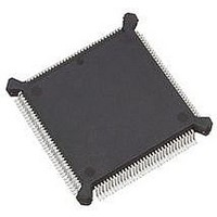
Manufacturer Part Number
MC68306EH16B
Description
IC MPU INTEGRATED 16MHZ 132-PQFP
Manufacturer
Freescale Semiconductor
Specifications of MC68306EH16B
Processor Type
M683xx 32-Bit
Speed
16MHz
Voltage
5V
Mounting Type
Surface Mount
Package / Case
132-MQFP, 132-PQFP
Controller Family/series
68K
Core Size
32 Bit
Cpu Speed
16.7MHz
No. Of Timers
1
Embedded Interface Type
UART
Digital Ic Case Style
PQFP
Supply Voltage Range
4.75V To 5.25V
Rohs Compliant
Yes
Lead Free Status / RoHS Status
Lead free / RoHS Compliant
Features
-
Available stocks
Company
Part Number
Manufacturer
Quantity
Price
Company:

Part Number:
MC68306EH16B
Manufacturer:
DATEL
Quantity:
87
Company:
Part Number:
MC68306EH16B
Manufacturer:
Freescale Semiconductor
Quantity:
10 000
Company:
Part Number:
MC68306EH16BR2
Manufacturer:
Freescale Semiconductor
Quantity:
10 000


5.2.7.1 DRAM REFRESH REGISTER. The refresh timer is a programmable period
counter that generates a refresh request every 16 to 4096 EXTAL periods, programmable
in 16 EXTAL period increments.
RR7–0—Refresh Rate Period
5.2.7.2 DRAM BANK CONFIGURATION REGISTER (HIGH HALF). The DRAM
configuration registers are not affected by any reset, and must be explicitly programmed.
This applies to both banks, whether used or not. Unused banks must be disabled to
prevent interference with other address decodes.
FFFFFFE4/5 (DR1), FFFFFFE0/1 (DR0)
DRA31–DRA17—DRAM Bank Address
DRW—DRAM Write
5-14
DRA31
RESE
15
T:
U
The value set in this field supplies the refresh rate for the DRAM controller. The refresh
rate can be calculated from the equation:
Where:
EXTAL is the crystal period in nanoseconds and period is in nanoseconds.
This bit field selects the base address for DRAM bank.
This bit determines whether write cycles are permitted to DRAM bank space. If read and
write cycles are both inhibited, the DRAM bank is inhibited.
Period = (16
0 = Write cycles are inhibited to DRAM bank space
1 = Write cycles are permitted to DRAM bank space
DRA3
14
0
U
DRA2
13
9
U
Never perform a TAS instruction to DRAM if the DRAM is
configured as write-only.
DRA2
12
8
U
(register value +1))
FFFFFFFC
DRA2
RESET
11
RR7
7
U
Freescale Semiconductor, Inc.
15
U
:
For More Information On This Product,
DRA2
10
6
U
RR6
14
U
MC68306 USER'S MANUAL
DRA2
Go to: www.freescale.com
9
5
U
RR5
13
U
DRA2
8
4
U
EXTAL
RR4
12
NOTE
U
DRA2
7
3
U
RR3
11
U
DRA2
U
6
2
RR2
10
U
SUPERVISOR ONLY
DRA21
5
U
RR1
U
9
DRA20
4
U
RR0
U
8
DRA19
3
U
DRA18
2
U
SUPERVISOR ONLY
MOTOROLA
DRA1
U
1
7
DRW
U
0
Related parts for MC68306EH16B
Image
Part Number
Description
Manufacturer
Datasheet
Request
R

Part Number:
Description:
Manufacturer:
Freescale Semiconductor, Inc
Datasheet:
Part Number:
Description:
Manufacturer:
Freescale Semiconductor, Inc
Datasheet:
Part Number:
Description:
Manufacturer:
Freescale Semiconductor, Inc
Datasheet:
Part Number:
Description:
Manufacturer:
Freescale Semiconductor, Inc
Datasheet:
Part Number:
Description:
Manufacturer:
Freescale Semiconductor, Inc
Datasheet:
Part Number:
Description:
Manufacturer:
Freescale Semiconductor, Inc
Datasheet:
Part Number:
Description:
Manufacturer:
Freescale Semiconductor, Inc
Datasheet:
Part Number:
Description:
Manufacturer:
Freescale Semiconductor, Inc
Datasheet:
Part Number:
Description:
Manufacturer:
Freescale Semiconductor, Inc
Datasheet:
Part Number:
Description:
Manufacturer:
Freescale Semiconductor, Inc
Datasheet:
Part Number:
Description:
Manufacturer:
Freescale Semiconductor, Inc
Datasheet:
Part Number:
Description:
Manufacturer:
Freescale Semiconductor, Inc
Datasheet:
Part Number:
Description:
Manufacturer:
Freescale Semiconductor, Inc
Datasheet:
Part Number:
Description:
Manufacturer:
Freescale Semiconductor, Inc
Datasheet:
Part Number:
Description:
Manufacturer:
Freescale Semiconductor, Inc
Datasheet: