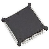
MC68306EH16B Freescale Semiconductor, MC68306EH16B Datasheet - Page 64

MC68306EH16B
Manufacturer Part Number
MC68306EH16B
Description
IC MPU INTEGRATED 16MHZ 132-PQFP
Manufacturer
Freescale Semiconductor
Specifications of MC68306EH16B
Processor Type
M683xx 32-Bit
Speed
16MHz
Voltage
5V
Mounting Type
Surface Mount
Package / Case
132-MQFP, 132-PQFP
Controller Family/series
68K
Core Size
32 Bit
Cpu Speed
16.7MHz
No. Of Timers
1
Embedded Interface Type
UART
Digital Ic Case Style
PQFP
Supply Voltage Range
4.75V To 5.25V
Rohs Compliant
Yes
Lead Free Status / RoHS Status
Lead free / RoHS Compliant
Features
-
Available stocks
Company
Part Number
Manufacturer
Quantity
Price
Company:
Part Number:
MC68306EH16B
Manufacturer:
DATEL
Quantity:
87
Company:
Part Number:
MC68306EH16B
Manufacturer:
Freescale Semiconductor
Quantity:
10 000
Company:
Part Number:
MC68306EH16BR2
Manufacturer:
Freescale Semiconductor
Quantity:
10 000
- Current page: 64 of 191
- Download datasheet (2Mb)
Freescale Semiconductor, Inc.
In a pseudo-asynchronous system, timing specifications allow DTACK to be asserted for a
read cycle before the data from a slave device is valid. The length of time that DTACK
may precede data is specified as parameter #31. This parameter must be met to ensure
the validity of the data latched into the processor. No maximum time is specified from the
assertion of AS to the assertion of DTACK. During this unlimited time, the processor
inserts wait cycles in one-clock-period increments until DTACK is recognized. Figure 3-30
shows the important timing parameters for a pseudo-asynchronous read cycle.
ADDR
11
AS
17
R/W
UDS/LDS
28
A
29
DATA
31
DTACK
Figure 3-30. Pseudo-Asynchronous Read Cycle
During a write cycle, after the processor asserts AS but before driving the data bus, the
processor drives R/W low. Parameter #55 specifies the minimum time between the
transition of R/W and the driving of the data bus, which is effectively the maximum turnoff
time for any device driving the data bus.
After the processor places valid data on the bus, it asserts the data strobe signal(s). A
data setup time, similar to the address setup time previously discussed, can be used to
improve performance. Parameter #26 is the minimum time a slave device can accept valid
data before recognizing a data strobe. The slave device asserts DTACK after it accepts
the data. Parameter #25 is the minimum time after negation of the strobes during which
the valid data remains on the address bus. Parameter #28 is the maximum time between
the negation of the strobes by the processor and the negation of DTACK by the slave
device. If DTACK remains asserted past the time specified by parameter #28, the
processor may recognize it as being asserted early in the next bus cycle and may
terminate that cycle prematurely. Figure 3-31 shows the important timing specifications for
a pseudo-asynchronous write cycle.
3-32
MC68306 USER'S MANUAL
MOTOROLA
For More Information On This Product,
Go to: www.freescale.com
Related parts for MC68306EH16B
Image
Part Number
Description
Manufacturer
Datasheet
Request
R
Part Number:
Description:
Manufacturer:
Freescale Semiconductor, Inc
Datasheet:
Part Number:
Description:
Manufacturer:
Freescale Semiconductor, Inc
Datasheet:
Part Number:
Description:
Manufacturer:
Freescale Semiconductor, Inc
Datasheet:
Part Number:
Description:
Manufacturer:
Freescale Semiconductor, Inc
Datasheet:
Part Number:
Description:
Manufacturer:
Freescale Semiconductor, Inc
Datasheet:
Part Number:
Description:
Manufacturer:
Freescale Semiconductor, Inc
Datasheet:
Part Number:
Description:
Manufacturer:
Freescale Semiconductor, Inc
Datasheet:
Part Number:
Description:
Manufacturer:
Freescale Semiconductor, Inc
Datasheet:
Part Number:
Description:
Manufacturer:
Freescale Semiconductor, Inc
Datasheet:
Part Number:
Description:
Manufacturer:
Freescale Semiconductor, Inc
Datasheet:
Part Number:
Description:
Manufacturer:
Freescale Semiconductor, Inc
Datasheet:
Part Number:
Description:
Manufacturer:
Freescale Semiconductor, Inc
Datasheet:
Part Number:
Description:
Manufacturer:
Freescale Semiconductor, Inc
Datasheet:
Part Number:
Description:
Manufacturer:
Freescale Semiconductor, Inc
Datasheet:
Part Number:
Description:
Manufacturer:
Freescale Semiconductor, Inc
Datasheet:


