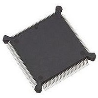
MC68306EH16B Freescale Semiconductor, MC68306EH16B Datasheet - Page 29

MC68306EH16B
Manufacturer Part Number
MC68306EH16B
Description
IC MPU INTEGRATED 16MHZ 132-PQFP
Manufacturer
Freescale Semiconductor
Specifications of MC68306EH16B
Processor Type
M683xx 32-Bit
Speed
16MHz
Voltage
5V
Mounting Type
Surface Mount
Package / Case
132-MQFP, 132-PQFP
Controller Family/series
68K
Core Size
32 Bit
Cpu Speed
16.7MHz
No. Of Timers
1
Embedded Interface Type
UART
Digital Ic Case Style
PQFP
Supply Voltage Range
4.75V To 5.25V
Rohs Compliant
Yes
Lead Free Status / RoHS Status
Lead free / RoHS Compliant
Features
-
Available stocks
Company
Part Number
Manufacturer
Quantity
Price
Company:
Part Number:
MC68306EH16B
Manufacturer:
DATEL
Quantity:
87
Company:
Part Number:
MC68306EH16B
Manufacturer:
Freescale Semiconductor
Quantity:
10 000
Company:
Part Number:
MC68306EH16BR2
Manufacturer:
Freescale Semiconductor
Quantity:
10 000
- Current page: 29 of 191
- Download datasheet (2Mb)
Freescale Semiconductor, Inc.
LW
2.1.15 Lower-Byte Write (
)
This signal is a combination of R/W low and LDS low for writing the lower-byte of a 16-bit
port. This signal simplifies memory system design by explicitly signalling that data is valid
on the lower portion of the data bus on a write operation. LW is also decoded for external
bus masters.
OE
2.1.16 Output Enable (
)
OE is a combination of R/ W high and an active data strobe (UDS or LDS ). OE is also
decoded for external bus masters.
RESET
2.1.17 Reset (
)
The external assertion of this bi-directional, open-drain signal can start a system
initialization sequence by resetting the processor. The processor assertion of RESET
(from executing a RESET instruction) resets all external devices of a system without
affecting the internal state of the processor. The interaction of internal and external
RESET , and the HALT signal is described in paragraph 3.5 Reset Operation.
2.2 CHIP SELECT SIGNALS
These eight three-state signals provide address decodes with programmable base and
range. CS7 –CS4 are only available in chip select mode (AMODE bit =1). CS3–CS0 are
always available.
2.3 DRAM CONTROLLER SIGNALS
The following signals are used to control an external DRAM for the MC68306.
CAS1
CAS0
2.3.1 Column Address Strobe (
–
)
These three-state signals provide column address strobe timing for external DRAM. CAS0
controls data lines D15–D8 and CAS1 controls D7–D0.
RAS1
RAS0
2.3.2 Row Address Strobe (
–
)
These three-state signals provide row address strobe timing for external DRAM. Each
RAS controls a separate bank of DRAM.
DRAMW
2.3.3 DRAM Write Signal (
)
This signal provides write control for external DRAM.
2.4 INTERRUPT CONTROL AND PARALLEL PORT SIGNALS
The following signals are used for interrupt control on the MC68306.
MOTOROLA
MC68306 USER'S MANUAL
2- 9
For More Information On This Product,
Go to: www.freescale.com
Related parts for MC68306EH16B
Image
Part Number
Description
Manufacturer
Datasheet
Request
R
Part Number:
Description:
Manufacturer:
Freescale Semiconductor, Inc
Datasheet:
Part Number:
Description:
Manufacturer:
Freescale Semiconductor, Inc
Datasheet:
Part Number:
Description:
Manufacturer:
Freescale Semiconductor, Inc
Datasheet:
Part Number:
Description:
Manufacturer:
Freescale Semiconductor, Inc
Datasheet:
Part Number:
Description:
Manufacturer:
Freescale Semiconductor, Inc
Datasheet:
Part Number:
Description:
Manufacturer:
Freescale Semiconductor, Inc
Datasheet:
Part Number:
Description:
Manufacturer:
Freescale Semiconductor, Inc
Datasheet:
Part Number:
Description:
Manufacturer:
Freescale Semiconductor, Inc
Datasheet:
Part Number:
Description:
Manufacturer:
Freescale Semiconductor, Inc
Datasheet:
Part Number:
Description:
Manufacturer:
Freescale Semiconductor, Inc
Datasheet:
Part Number:
Description:
Manufacturer:
Freescale Semiconductor, Inc
Datasheet:
Part Number:
Description:
Manufacturer:
Freescale Semiconductor, Inc
Datasheet:
Part Number:
Description:
Manufacturer:
Freescale Semiconductor, Inc
Datasheet:
Part Number:
Description:
Manufacturer:
Freescale Semiconductor, Inc
Datasheet:
Part Number:
Description:
Manufacturer:
Freescale Semiconductor, Inc
Datasheet:


