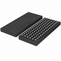
SSTUB32866EC/G,518 NXP Semiconductors, SSTUB32866EC/G,518 Datasheet - Page 12

SSTUB32866EC/G,518
Manufacturer Part Number
SSTUB32866EC/G,518
Description
IC REG BUFFER 25BIT 96-LFBGA
Manufacturer
NXP Semiconductors
Datasheet
1.SSTUB32866ECG518.pdf
(30 pages)
Specifications of SSTUB32866EC/G,518
Logic Type
1:1, 1:2 Configurable Registered Buffer with Parity
Package / Case
96-LFBGA
Supply Voltage
1.7 V ~ 2 V
Number Of Bits
25, 14
Operating Temperature
0°C ~ 70°C
Mounting Type
Surface Mount
Logic Family
SSTU
Number Of Circuits
1
Maximum Clock Frequency
450 MHz
Propagation Delay Time
1.5 ns
High Level Output Current
- 8 mA
Low Level Output Current
8 mA
Supply Voltage (max)
2 V
Maximum Operating Temperature
+ 70 C
Minimum Operating Temperature
0 C
Mounting Style
SMD/SMT
Supply Voltage (min)
1.7 V
Lead Free Status / RoHS Status
Lead free / RoHS Compliant
Lead Free Status / RoHS Status
Lead free / RoHS Compliant, Lead free / RoHS Compliant
Other names
568-3543-2
935281279518
SSTUB32866EC/G-T
935281279518
SSTUB32866EC/G-T
Available stocks
Company
Part Number
Manufacturer
Quantity
Price
Company:
Part Number:
SSTUB32866EC/G,518
Manufacturer:
NXP Semiconductors
Quantity:
10 000
NXP Semiconductors
10. Characteristics
Table 8.
At recommended operating conditions (see
SSTUB32866_4
Product data sheet
Symbol
V
V
I
I
I
C
Input RESET
V
V
I
I
I
DD
DDD
I
L
OH
OL
IL
IH
i
Characteristics
Parameter
HIGH-level output voltage
LOW-level output voltage
input current
supply current
dynamic operating current
per MHz
input capacitance
LOW-level input voltage
HIGH-level input voltage
input current
leakage current
All information provided in this document is subject to legal disclaimers.
I
all inputs; V
static Standby mode; RESET = GND;
Conditions
I
I
static Operating mode; RESET = V
I
V
clock only; RESET = V
V
switching at 50 % duty cycle; I
V
per each data input, 1 : 1 mode;
RESET = V
CK and CK switching at 50 % duty
cycle; one data input switching at half
clock frequency, 50 % duty cycle;
I
per each data input, 1 : 2 mode;
RESET = V
CK and CK switching at 50 % duty
cycle; one data input switching at half
clock frequency, 50 % duty cycle;
I
data and CSR inputs;
V
CK and CK inputs; V
V
RESET input; V
V
V
V
Table
OH
OL
O
O
O
O
I
I
DD
I
i(p-p)
DD
I
I
= 0 mA; V
= 0 mA; V
= V
= V
= 0 mA; V
= 0 mA; V
= V
= V
= V
= 6 mA; V
= −6 mA; V
= 1.8 V
= 1.8 V
IH(AC)
IH(AC)
ref
= 600 mV; V
DD
SS
7); unless otherwise specified.
Rev. 04 — 15 April 2010
± 250 mV; V
I
DD
DD
or V
or V
DD
DD
DD
DD
= V
1.8 V DDR2-800 configurable registered buffer with parity
DD
; V
; V
DD
= 2.0 V
= 2.0 V;
= 1.8 V
= 1.8 V
I
IL(AC)
IL(AC)
DD
= 1.7 V
I
I
= V
= V
= V
= 1.7 V
DD
or GND; V
DD
ICR
; CK and CK
DD
IH(AC)
IH(AC)
= 1.8 V
DD
or GND;
= 1.8 V
= 0.9 V;
;
or V
or V
DD
O
IL(AC)
IL(AC)
= 0 mA;
= 2.0 V
DD
;
;
;
Min
1.2
-
-
-
-
-
-
-
2.5
2
3
−0.5
0.7V
−5
−100
DD
SSTUB32866
Typ
-
-
-
-
-
16
11
19
-
-
-
-
-
-
−25
© NXP B.V. 2010. All rights reserved.
Max
-
0.5
±5
2
40
-
-
-
3.5
3
4
+0.3V
2.5
+5
−10
DD
12 of 30
Unit
V
V
μA
mA
mA
μA
μA
μA
pF
pF
pF
V
V
μA
μA


