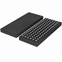
SSTUB32866EC/G,518 NXP Semiconductors, SSTUB32866EC/G,518 Datasheet - Page 7

SSTUB32866EC/G,518
Manufacturer Part Number
SSTUB32866EC/G,518
Description
IC REG BUFFER 25BIT 96-LFBGA
Manufacturer
NXP Semiconductors
Datasheet
1.SSTUB32866ECG518.pdf
(30 pages)
Specifications of SSTUB32866EC/G,518
Logic Type
1:1, 1:2 Configurable Registered Buffer with Parity
Package / Case
96-LFBGA
Supply Voltage
1.7 V ~ 2 V
Number Of Bits
25, 14
Operating Temperature
0°C ~ 70°C
Mounting Type
Surface Mount
Logic Family
SSTU
Number Of Circuits
1
Maximum Clock Frequency
450 MHz
Propagation Delay Time
1.5 ns
High Level Output Current
- 8 mA
Low Level Output Current
8 mA
Supply Voltage (max)
2 V
Maximum Operating Temperature
+ 70 C
Minimum Operating Temperature
0 C
Mounting Style
SMD/SMT
Supply Voltage (min)
1.7 V
Lead Free Status / RoHS Status
Lead free / RoHS Compliant
Lead Free Status / RoHS Status
Lead free / RoHS Compliant, Lead free / RoHS Compliant
Other names
568-3543-2
935281279518
SSTUB32866EC/G-T
935281279518
SSTUB32866EC/G-T
Available stocks
Company
Part Number
Manufacturer
Quantity
Price
Company:
Part Number:
SSTUB32866EC/G,518
Manufacturer:
NXP Semiconductors
Quantity:
10 000
NXP Semiconductors
Table 3.
[1]
[2]
SSTUB32866_4
Product data sheet
Symbol
GND
V
VREF
CK
CK
C0
C1
RESET
CSR
DCS
D1 to D25
DODT
DCKE
PAR_IN
Q1 to Q25,
Q2A to Q14A,
Q1B to Q14B
PPO
QCS, QCSA,
QCSB
QODT, QODTA,
QODTB
QCKE,
QCKEA,
QCKEB
QERR
n.c.
DNU
DD
Data inputs = D2, D3, D5, D6, D8 to D25 when C0 = 0 and C1 = 0.
Data inputs = D2, D3, D5, D6, D8 to D14 when C0 = 0 and C1 = 1.
Data inputs = D1 to D6, D8 to D10, D12, D13 when C0 = 1 and C1 = 1.
Depends on configuration. See
Pin description
Pin
H3, H4, K3, K4, M3,
M4, P3, P4
A4, C3, C4, E3, E4,
G3, G4, J3, J4, L3, L4,
N3, N4, R3, R4, T4
H1
J1
G6
G5
G2
J2
H2
[2]
[2]
[2]
[2]
A2
[2]
[2]
[2]
D2
[2]
[2]
B3, B4, D3, D4, F3, F4,
A3, T3
G1
6.2 Pin description
Figure
4,
Figure
All information provided in this document is subject to legal disclaimers.
LVCMOS inputs
LVCMOS input
Type
ground input
1.8 V nominal
0.9 V nominal
differential input
differential input
SSTL_18 input
SSTL_18 input
SSTL_18 input
SSTL_18 input
SSTL_18 input
1.8 V CMOS
outputs
1.8 V CMOS
output
1.8 V CMOS
output
1.8 V CMOS
output
1.8 V CMOS
output
open-drain
output
-
-
5, and
Rev. 04 — 15 April 2010
Figure 6
1.8 V DDR2-800 configurable registered buffer with parity
for ball number.
Description
ground
power supply voltage
input reference voltage
positive master clock input
negative master clock input
Configuration control inputs; Register A or Register B and
1 : 1 mode or 1 : 2 mode select.
Asynchronous reset input (active LOW). Resets registers and
disables VREF data and clock.
Chip select inputs (active LOW). Disables D1 to D25
outputs switching when both inputs are HIGH.
Data input. Clocked in on the crossing of the rising edge of
CK and the falling edge of CK.
The outputs of this register bit will not be suspended by the
DCS and CSR control.
The outputs of this register bit will not be suspended by the
DCS and CSR control.
Parity input. Arrives one clock cycle after the corresponding
data input.
Data outputs that are suspended by the DCS and CSR
control.
Partial parity out. Indicates odd parity of inputs D1 to D25.
Data output that will not be suspended by the DCS and CSR
control.
Data output that will not be suspended by the DCS and CSR
control.
Data output that will not be suspended by the DCS and CSR
control.
Output error bit (active LOW). Generated one clock cycle
after the corresponding data output.
Not connected. Ball present but no internal connection to the
die.
Do not use. Inputs are in standby-equivalent mode and
outputs are driven LOW.
[3]
SSTUB32866
© NXP B.V. 2010. All rights reserved.
[1]
7 of 30
[1]


