SSTUB32866EC/G,518 NXP Semiconductors, SSTUB32866EC/G,518 Datasheet - Page 30
SSTUB32866EC/G,518
Manufacturer Part Number
SSTUB32866EC/G,518
Description
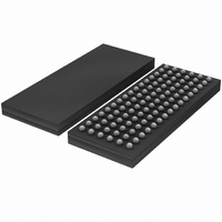
IC REG BUFFER 25BIT 96-LFBGA
Manufacturer
NXP Semiconductors
Datasheet
1.SSTUB32866ECG518.pdf
(30 pages)
Specifications of SSTUB32866EC/G,518
Logic Type
1:1, 1:2 Configurable Registered Buffer with Parity
Package / Case
96-LFBGA
Supply Voltage
1.7 V ~ 2 V
Number Of Bits
25, 14
Operating Temperature
0°C ~ 70°C
Mounting Type
Surface Mount
Logic Family
SSTU
Number Of Circuits
1
Maximum Clock Frequency
450 MHz
Propagation Delay Time
1.5 ns
High Level Output Current
- 8 mA
Low Level Output Current
8 mA
Supply Voltage (max)
2 V
Maximum Operating Temperature
+ 70 C
Minimum Operating Temperature
0 C
Mounting Style
SMD/SMT
Supply Voltage (min)
1.7 V
Lead Free Status / RoHS Status
Lead free / RoHS Compliant
Lead Free Status / RoHS Status
Lead free / RoHS Compliant, Lead free / RoHS Compliant
Other names
568-3543-2
935281279518
SSTUB32866EC/G-T
935281279518
SSTUB32866EC/G-T
Available stocks
Company
Part Number
Manufacturer
Quantity
Price
Company:

Part Number:
SSTUB32866EC/G,518
Manufacturer:
NXP Semiconductors
Quantity:
10 000


NXP Semiconductors
18. Contents
1
2
3
4
4.1
5
6
6.1
6.2
7
7.1
8
9
10
10.1
11
11.1
11.2
11.3
11.4
12
13
13.1
13.2
13.3
13.4
14
15
16
16.1
16.2
16.3
16.4
17
18
General description . . . . . . . . . . . . . . . . . . . . . . 1
Features and benefits . . . . . . . . . . . . . . . . . . . . 1
Applications . . . . . . . . . . . . . . . . . . . . . . . . . . . . 1
Ordering information . . . . . . . . . . . . . . . . . . . . . 2
Functional diagram . . . . . . . . . . . . . . . . . . . . . . 3
Pinning information . . . . . . . . . . . . . . . . . . . . . . 5
Functional description . . . . . . . . . . . . . . . . . . . 8
Limiting values. . . . . . . . . . . . . . . . . . . . . . . . . 10
Recommended operating conditions. . . . . . . 11
Characteristics . . . . . . . . . . . . . . . . . . . . . . . . . 12
Test information . . . . . . . . . . . . . . . . . . . . . . . . 17
Package outline . . . . . . . . . . . . . . . . . . . . . . . . 23
Soldering of SMD packages . . . . . . . . . . . . . . 24
Abbreviations . . . . . . . . . . . . . . . . . . . . . . . . . . 26
Revision history . . . . . . . . . . . . . . . . . . . . . . . . 27
Legal information. . . . . . . . . . . . . . . . . . . . . . . 28
Contact information. . . . . . . . . . . . . . . . . . . . . 29
Contents . . . . . . . . . . . . . . . . . . . . . . . . . . . . . . 30
data output load circuit . . . . . . . . . . . . . . . . . . 17
information . . . . . . . . . . . . . . . . . . . . . . . . . . . 19
measurement information . . . . . . . . . . . . . . . . 20
measurement information . . . . . . . . . . . . . . . . 21
Wave and reflow soldering . . . . . . . . . . . . . . . 24
Ordering options . . . . . . . . . . . . . . . . . . . . . . . . 2
Pinning . . . . . . . . . . . . . . . . . . . . . . . . . . . . . . . 5
Pin description . . . . . . . . . . . . . . . . . . . . . . . . . 7
Function table . . . . . . . . . . . . . . . . . . . . . . . . . . 9
Timing diagrams . . . . . . . . . . . . . . . . . . . . . . . 14
Parameter measurement information for
Data output slew rate measurement
Error output load circuit and voltage
Partial parity out load circuit and voltage
Introduction to soldering . . . . . . . . . . . . . . . . . 24
Wave soldering . . . . . . . . . . . . . . . . . . . . . . . . 24
Reflow soldering . . . . . . . . . . . . . . . . . . . . . . . 25
Data sheet status . . . . . . . . . . . . . . . . . . . . . . 28
Definitions . . . . . . . . . . . . . . . . . . . . . . . . . . . . 28
Disclaimers . . . . . . . . . . . . . . . . . . . . . . . . . . . 28
Trademarks. . . . . . . . . . . . . . . . . . . . . . . . . . . 29
1.8 V DDR2-800 configurable registered buffer with parity
Please be aware that important notices concerning this document and the product(s)
described herein, have been included in section ‘Legal information’.
© NXP B.V. 2010.
For more information, please visit: http://www.nxp.com
For sales office addresses, please send an email to: salesaddresses@nxp.com
SSTUB32866
Document identifier: SSTUB32866_4
Date of release: 15 April 2010
All rights reserved.
Related parts for SSTUB32866EC/G,518
Image
Part Number
Description
Manufacturer
Datasheet
Request
R

Part Number:
Description:
NXP Semiconductors designed the LPC2420/2460 microcontroller around a 16-bit/32-bitARM7TDMI-S CPU core with real-time debug interfaces that include both JTAG andembedded trace
Manufacturer:
NXP Semiconductors
Datasheet:

Part Number:
Description:
NXP Semiconductors designed the LPC2458 microcontroller around a 16-bit/32-bitARM7TDMI-S CPU core with real-time debug interfaces that include both JTAG andembedded trace
Manufacturer:
NXP Semiconductors
Datasheet:
Part Number:
Description:
NXP Semiconductors designed the LPC2468 microcontroller around a 16-bit/32-bitARM7TDMI-S CPU core with real-time debug interfaces that include both JTAG andembedded trace
Manufacturer:
NXP Semiconductors
Datasheet:
Part Number:
Description:
NXP Semiconductors designed the LPC2470 microcontroller, powered by theARM7TDMI-S core, to be a highly integrated microcontroller for a wide range ofapplications that require advanced communications and high quality graphic displays
Manufacturer:
NXP Semiconductors
Datasheet:
Part Number:
Description:
NXP Semiconductors designed the LPC2478 microcontroller, powered by theARM7TDMI-S core, to be a highly integrated microcontroller for a wide range ofapplications that require advanced communications and high quality graphic displays
Manufacturer:
NXP Semiconductors
Datasheet:
Part Number:
Description:
The Philips Semiconductors XA (eXtended Architecture) family of 16-bit single-chip microcontrollers is powerful enough to easily handle the requirements of high performance embedded applications, yet inexpensive enough to compete in the market for hi
Manufacturer:
NXP Semiconductors
Datasheet:
Part Number:
Description:
The XA-S3 device is a member of Philips Semiconductors? XA(eXtended Architecture) family of high performance 16-bitsingle-chip microcontrollers
Manufacturer:
NXP Semiconductors
Datasheet:

Part Number:
Description:
The NXP BlueStreak LH75401/LH75411 family consists of two low-cost 16/32-bit System-on-Chip (SoC) devices
Manufacturer:
NXP Semiconductors
Datasheet:
Part Number:
Description:
The NXP LPC3130/3131 combine an 180 MHz ARM926EJ-S CPU core, high-speed USB2
Manufacturer:
NXP Semiconductors
Datasheet:
Part Number:
Description:
The NXP LPC3141 combine a 270 MHz ARM926EJ-S CPU core, High-speed USB 2
Manufacturer:
NXP Semiconductors
Part Number:
Description:
The NXP LPC3143 combine a 270 MHz ARM926EJ-S CPU core, High-speed USB 2
Manufacturer:
NXP Semiconductors

Part Number:
Description:
The NXP LPC3152 combines an 180 MHz ARM926EJ-S CPU core, High-speed USB 2
Manufacturer:
NXP Semiconductors
Part Number:
Description:
The NXP LPC3154 combines an 180 MHz ARM926EJ-S CPU core, High-speed USB 2
Manufacturer:
NXP Semiconductors

Part Number:
Description:
Standard level N-channel enhancement mode Field-Effect Transistor (FET) in a plastic package using NXP High-Performance Automotive (HPA) TrenchMOS technology
Manufacturer:
NXP Semiconductors
Datasheet: