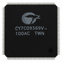
CY7C09569V-100AC Cypress Semiconductor Corp, CY7C09569V-100AC Datasheet - Page 6

CY7C09569V-100AC
Manufacturer Part Number
CY7C09569V-100AC
Description
IC SRAM 576KBIT 100MHZ 144LQFP
Manufacturer
Cypress Semiconductor Corp
Specifications of CY7C09569V-100AC
Format - Memory
RAM
Memory Type
SRAM - Dual Port, Synchronous
Memory Size
576K (16K x 36)
Speed
100MHz
Interface
Parallel
Voltage - Supply
3 V ~ 3.6 V
Operating Temperature
0°C ~ 70°C
Package / Case
144-LQFP
Density
576Kb
Access Time (max)
12.5ns
Sync/async
Synchronous
Architecture
SDR
Clock Freq (max)
67MHz
Operating Supply Voltage (typ)
3.3V
Address Bus
14b
Package Type
TQFP
Operating Temp Range
0C to 70C
Number Of Ports
2
Supply Current
385mA
Operating Supply Voltage (min)
3.135V
Operating Supply Voltage (max)
3.465V
Operating Temperature Classification
Commercial
Mounting
Surface Mount
Pin Count
144
Word Size
36b
Number Of Words
16K
Lead Free Status / RoHS Status
Contains lead / RoHS non-compliant
Other names
428-1189
Available stocks
Company
Part Number
Manufacturer
Quantity
Price
Company:
Part Number:
CY7C09569V-100AC
Manufacturer:
Cypress Semiconductor Corp
Quantity:
10 000
Part Number:
CY7C09569V-100AC
Manufacturer:
CYP
Quantity:
20 000
Maximum Ratings
(Above which the useful life may be impaired. For user guide-
lines, not tested.)
Storage Temperature ................................. –65 C to +150 C
Ambient Temperature with
Power Applied.............................................–55 C to +125 C
Supply Voltage to Ground Potential ............... –0.5V to +4.6V
DC Voltage Applied to
Outputs in High Z State ...........................–0.5V to V
DC Input Voltage...................................–0.5V to V
Electrical Characteristics
Capacitance
Note:
Document #: 38-06054 Rev. *A
V
V
V
V
I
I
I
I
I
I
4.
5.
Parameter
C
C
OZ
CC
SB1
SB2
SB3
SB4
OH
OL
IH
IL
IN
OUT
The voltage on any input or I/O pin can not exceed the power pin during power-up.
Pulse width < 20 ns.
Parameter
Output HIGH Voltage
(V
Output LOW Voltage
(V
Input HIGH Voltage
Input LOW Voltage
Output Leakage Current
Operating Current (V
I
Standby Current (Both Ports TTL
Level) CE
Standby Current (One Port TTL
Level) CE
Standby Current (Both Ports
CMOS Level)
CE
Standby Current (One Port
CMOS Level)
CE
OUT
DD
DD
L
L
& CE
| CE
= 0 mA) Outputs Disabled
= Min., I
= Min., I
R
L
L
R
[4]
& CE
| CE
V
OH
OL
V
IH
DD
Input Capacitance
Output Capacitance
= +4.0 mA)
R
, f = f
= –4.0 mA)
R
– 0.2V, f = 0
Description
V
Over the Operating Range
V
DD
IH
MAX
IH
, f = f
Description
, f = f
= Max.,
MAX
MAX
Commercial
Industrial
Commercial
Industrial
Commercial
Industrial
Commercial
Industrial
Commercial
Industrial
DD
DD
+0.5V
+0.5V
[5]
T
V
A
DD
= 25 C, f = 1 MHz,
= 3.3V
Min. Typ. Max. Min. Typ. Max. Min. Typ. Max.
–10
2.4
2.0
Test Conditions
Output Current into Outputs (LOW)............................. 20 mA
Static Discharge Voltage ........................................... >2001V
Latch-Up Current..................................................... >200 mA
Operating Range
Commercial
Industrial
0.01
-100
250
170
150
Range
30
385
220
200
0.4
0.8
10
75
1
–10
2.4
2.0
CY7C09569V
CY7C09579V
–40 C to +85 C
Temperature
0 C to +70 C
0.01
0.01
240
270
160
170
140
150
-83
25
35
Ambient
360
385
210
235
190
200
0.4
0.8
Max.
10
70
85
1
1
10
10
–10
2.4
2.0
CY7C09569V
CY7C09579V
0.01
230
150
130
-67
25
3.3V
3.3V
Page 6 of 30
Unit
340
200
180
V
0.4
0.8
10
65
pF
pF
1
DD
165 mV
165 mV
Unit
mA
mA
mA
mA
mA
mA
mA
mA
mA
mA
V
V
V
V
A


