PCF8534AH/1,518 NXP Semiconductors, PCF8534AH/1,518 Datasheet
PCF8534AH/1,518
Specifications of PCF8534AH/1,518
PCF8534AH/1-T
PCF8534AH/1-T
Available stocks


Related parts for PCF8534AH/1,518


PCF8534AH/1,518 Summary of contents
Page 1
PCF8534A Universal LCD driver for low multiplex rates Rev. 03 — 10 November 2008 1. General description The PCF8534A is a peripheral device which interfaces to almost any LCD with low multiplex rates. It generates the drive signals for any ...
Page 2
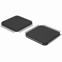
... NXP Semiconductors 3. Ordering information Table 1. Ordering information Type number Package Name PCF8534AH/1 LQFP80 PCF8534AU/DA/1 PCF8534AU 4. Marking Table 2. Type number PCF8534AH/1 PCF8534AU/DA/1 5. Block diagram V LCD LCD BIAS GENERATOR V SS CLK CLOCK SELECT AND TIMING SYNC OSC OSCILLATOR SCL INPUT FILTERS SDA Fig 1. ...
Page 3
... NXP Semiconductors 6. Pinning information 6.1 Pinning S31 S32 S33 S34 S35 S36 S37 S38 S39 S40 S41 S42 S43 S44 S45 S46 S47 S48 S49 S50 Fig 2. PCF8534A_3 Product data sheet PCF8534AH Top view. For mechanical details, see Figure PCF8534AH/1 pin configuration (SOT315-1) Rev. 03 — ...
Page 4
... NXP Semiconductors Fig 3. PCF8534A_3 Product data sheet C1 S51 64 65 S52 66 S53 S54 67 68 S55 69 S56 70 S57 71 S58 72 S59 73 BP0 74 BP1 BP2 75 76 BP3 SDA 1 2 SCL CLK 3 F For mechanical details, see Figure 24. PCF8534AU/DA/1 pin configuration (bare die) Rev. 03 — 10 November 2008 ...
Page 5
... NXP Semiconductors 6.2 Pin description Table 3. Symbol S31 to S59 BP0 to BP3 n.c. SDA SCL CLK V DD SYNC OSC SA0 LCD S0 to S30 [1] The substrate (rear side of the die) is wired Functional description The PCF8534A is a versatile peripheral device designed to interface any microprocessor or microcontroller to a wide variety of LCDs ...
Page 6
... NXP Semiconductors Fig 4. The host microprocessor or microcontroller maintains the 2-line I channel with the PCF8534A. Biasing voltages for the multiplexed LCD waveforms are generated internally, removing the need for an external bias generator. The internal oscillator is selected by connecting pin OSC to V power supplies (pins V 7 ...
Page 7
... NXP Semiconductors Table 5 together with the biasing characteristics as functions of V discrimination ratios (D). A practical value for V threshold voltage (V the static drive mode a suitable choice is V Multiplex drive ratios of 1:3 and 1:4 with hence the contrast ratios are smaller e.g 1.732 The advantage of these modes is the reduction of the LCD full-scale voltage V follows: • ...
Page 8
... NXP Semiconductors 7.4 LCD drive mode waveforms 7.4.1 Static drive mode The static LCD drive mode is used when a single backplane is provided in the LCD. Backplane and segment drive waveforms for this mode are shown in Fig 5. PCF8534A_3 Product data sheet V LCD BP0 V SS ...
Page 9
... NXP Semiconductors 7.4.2 1:2 Multiplex drive mode When two backplanes are provided in the LCD, the 1:2 multiplex mode applies. The PCF8534A allows the use of Figure 7. Fig 6. PCF8534A_3 Product data sheet 1 1 bias LCD BP0 LCD LCD BP1 LCD LCD LCD Sn+1 ...
Page 10
... NXP Semiconductors Fig 7. PCF8534A_3 Product data sheet V LCD LCD BP0 LCD LCD LCD BP1 LCD LCD LCD LCD LCD LCD S n LCD LCD LCD LCD state LCD LCD V LCD V LCD LCD LCD 0 V state LCD LCD V LCD V ( (t) V (t). state1 Sn BP0 ...
Page 11
... NXP Semiconductors 7.4.3 1:3 Multiplex drive mode When three backplanes are provided in the LCD, the 1:3 multiplex drive mode applies, as shown in Fig 8. PCF8534A_3 Product data sheet Figure 8. V LCD LCD BP0 LCD LCD LCD BP1 LCD LCD LCD BP2 LCD V SS ...
Page 12
... NXP Semiconductors 7.4.4 1:4 Multiplex drive mode When four backplanes are provided in the LCD, the 1:4 multiplex drive mode applies, as shown in BP0 BP1 BP2 BP3 Sn Sn+1 Sn+2 Sn+3 state 1 state 2 Fig 9. PCF8534A_3 Product data sheet Figure 9. V LCD LCD LCD V SS ...
Page 13
... NXP Semiconductors 7.5 Oscillator The internal logic and the LCD drive signals of the PCF8534A are timed by the frequency f , which equals either the built-in oscillator frequency f clk f . The clock frequency f clk(ext) 7.5.1 Internal clock The internal oscillator is enabled by connecting pin OSC to pin V output from pin CLK is the clock signal for any cascaded PCF8534A in the system ...
Page 14
... NXP Semiconductors 7.9 Backplane outputs The LCD drive section includes four backplane outputs: BP0 to BP3. The backplane output signals are generated based on the selected LCD drive mode. • In 1:4 multiplex drive mode: BP0 to BP3 must be connected directly to the LCD. If less than four backplane outputs are required the unused outputs can be left as an open-circuit. • ...
Page 15
... NXP Semiconductors The following applies to • Static drive mode: the eight transmitted data bits are placed in row 0 to eight successive display RAM addresses. • 1:2 multiplex drive mode: the eight transmitted data bits are placed in row 0 and 1 to four successive display RAM addresses. ...
Page 16
LCD segments LCD backplanes a S n+2 b BP0 n static n n+6 BP0 1 ...
Page 17
... NXP Semiconductors 7.12 Subaddress counter The storage of display data is conditioned by the contents of the subaddress counter. Storage is allowed only when the contents of the subaddress counter agree with the hardware subaddress applied to A0, A1 and A2. The subaddress counter value is defined by the device select command (see and the hardware subaddress do not agree then data storage is blocked but the data pointer will be incremented as if data storage had taken place ...
Page 18
... NXP Semiconductors 7.15 Blinker The display blinking capabilities of the PCF8534A are very versatile. The whole display can be blinked at frequencies set by the blink select command (see blinking frequencies are fractions of the clock frequency. The ratios between the clock and blinking frequencies depend on the mode in which the device is operating (see Table 7 ...
Page 19
... NXP Semiconductors Fig 12. Bit transfer 8.1.1.1 START and STOP conditions Both data and clock lines remain HIGH when the bus is not busy. A HIGH-to-LOW change of the data line, while the clock is HIGH, is defined as the START condition (S). A LOW-to-HIGH change of the data line, while the clock is HIGH, is defined as the STOP condition (P) ...
Page 20
... NXP Semiconductors • A slave receiver which is addressed must generate an acknowledge after the reception of each byte. • A master receiver must generate an acknowledge after the reception of each byte that has been clocked out of the slave transmitter. • The device that acknowledges must pull-down the SDA line during the acknowledge ...
Page 21
... NXP Semiconductors 2 8.2 I C-bus protocol 2 Two I C-bus slave addresses (0111 000 and 0111 001) are reserved for the PCF8534A. The least significant bit of the slave address is bit R/W. The PCF8534A is a write-only device. It will not respond to a read access, so this bit should always be logic 0. The second bit of the slave address is defi ...
Page 22
... NXP Semiconductors R slave address control byte EXAMPLES a) transmit two bytes of RAM data transmit two command bytes transmit one command byte and two RAM date bytes Fig 17. I C-bus protocol 8.3 Command decoder The command decoder identifies command bytes that arrive on the I fi ...
Page 23
... NXP Semiconductors Table 10. Bit Table 11. See Section Bit Table 12. See Section Bit Table 13. See Section Bit [1] The bank select command has no effect in 1:3 or 1:4 multiplex drive modes. PCF8534A_3 Product data sheet Mode set command bit description Symbol Value Description M[1:0] LCD drive mode selection 01 static ...
Page 24
... NXP Semiconductors Table 14. See Section Bit [1] Only normal blinking can be selected in multiplexer 1:3 or 1:4 drive modes. 8.4 Display controller The display controller executes the commands identified by the command decoder. It contains the status registers of the PCF8534A and coordinates their effects. The controller also loads display data into the display RAM as required by the storage order ...
Page 25
... NXP Semiconductors 9. Internal circuitry Fig 18. Device protection diagram PCF8534A_3 Product data sheet Universal LCD driver for low multiplex rates V DD SA0 CLK OSC SYNC A0, A1 LCD BP0, BP1, BP2, BP3 LCD S0 to S59 V SS Rev. 03 — 10 November 2008 PCF8534A SCL V SS ...
Page 26
... NXP Semiconductors 10. Limiting values CAUTION Static voltages across the liquid crystal display can build up when the LCD supply voltage (V LCD display artifacts. To avoid such artifacts, V Table 15. In accordance with the Absolute Maximum Rating System (IEC 60134). Symbol LCD I DD(LCD tot P/out ...
Page 27
... NXP Semiconductors 11. Static characteristics Table 16. Static characteristics Symbol Parameter Supplies V supply voltage DD V LCD supply voltage LCD I supply current DD I LCD supply current DD(LCD) Logic V input voltage I V LOW-level input voltage IL V HIGH-level input voltage IH V power-on reset voltage POR ...
Page 28
... NXP Semiconductors 12. Dynamic characteristics Table 17. Dynamic characteristics Symbol Parameter Clock Internal: output pin CLK f oscillator frequency osc External: input pin CLK f external clock frequency clk(ext) t HIGH-level clock time clk(H) t LOW-level clock time clk(L) Synchronization: input pin SYNC t SYNC propagation delay ...
Page 29
... NXP Semiconductors BP0 to BP3, and S0 to S59 Fig 19. Driver timing waveforms SDA SCL SDA Fig 20. I PCF8534A_3 Product data sheet clk t clk(H) CLK SYNC t PD(SYNC_N BUF LOW t HD;STA C-bus timing waveforms Rev. 03 — 10 November 2008 PCF8534A Universal LCD driver for low multiplex rates ...
Page 30
... NXP Semiconductors 13. Application information 13.1 Cascaded operation Large display configurations PCF8534As can be recognized on the same 2 I C-bus by using the 3-bit hardware subaddress (A0, A1 and A2) and the programmable 2 I C-bus slave address (SA0). Table 18. Cluster cascaded PCF8534As are synchronized, they can share the backplane signals from one of the devices in the cascade ...
Page 31
... NXP Semiconductors V LCD HOST MICRO- PROCESSOR/ MICRO- CONTROLLER V SS Fig 21. Cascaded PCF8534A configuration The SYNC line is provided to maintain the correct synchronization between all cascaded PCF8534As. Synchronization is guaranteed after a power-on reset. The only time that SYNC is likely to be needed is if synchronization is accidentally lost (e.g. by noise in adverse electrical environments or by defi ...
Page 32
... NXP Semiconductors Fig 22. Synchronization of the cascade for various PCF8534A drive modes The contact resistance between the SYNC pins of cascaded devices must be controlled. If the resistance is too high, the device will not be able to synchronize properly. Table 19 Table 19. Number of devices PCF8534A_3 Product data sheet ...
Page 33
... NXP Semiconductors 14. Package outline LQFP80: plastic low profile quad flat package; 80 leads; body 1 pin 1 index DIMENSIONS (mm are the original dimensions) A UNIT max. 0.16 1.5 mm 1.6 0.25 0.04 1.3 Note 1. Plastic or metal protrusions of 0.25 mm maximum per side are not included. OUTLINE VERSION ...
Page 34
... NXP Semiconductors 15. Bare die outline Wire bond die; 76 bonding pads; 2.91 x 2. DIMENSIONS (mm are the original dimensions) UNIT max mm nom 0.38 2.91 2.62 min Notes 1. Pad size 2. Passivation opening 3. Marking code OUTLINE VERSION IEC PCF8534AU Fig 24. PCF8534AU die outline PCF8534A_3 ...
Page 35
... NXP Semiconductors Table 20. Symbol SDA SCL CLK V DD SYNC OSC SA0 LCD S10 S11 S12 S13 S14 S15 S16 S17 S18 S19 S20 S21 S22 S23 S24 S25 S26 S27 PCF8534A_3 Product data sheet Bonding pad locations [1] Pad Coordinates 1384.4 280 2 1384 ...
Page 36
... NXP Semiconductors Table 20. Symbol S28 S29 S30 S31 S32 S33 S34 S35 S36 S37 S38 S39 S40 S41 S42 S43 S44 S45 S46 S47 S48 S49 S50 S51 S52 S53 S54 S55 S56 S57 S58 S59 BP0 BP1 BP2 BP3 [1] All coordinates are referenced the center of the die (see ...
Page 37
... NXP Semiconductors Fig 25. Alignment marks Table 21. Symbol [1] All coordinates are referenced the center of the die (see 16. Handling information Inputs and outputs are protected against electrostatic discharge in normal handling. However completely safe you must take normal precautions appropriate to handling MOS devices; see JESD625-A and/or IEC61340-5 . ...
Page 38
... NXP Semiconductors 17. Packing information Fig 26. Tray details for PCF8534AU/DA/1 Fig 27. Tray alignment for PCF8534AU/DA/1 PCF8534A_3 Product data sheet 1.1 2.1 3.1 1.2 2.2 1 Rev. 03 — 10 November 2008 PCF8534A Universal LCD driver for low multiplex rates A x.1 E PC8534A-1 001aai650 © NXP B.V. 2008. All rights reserved. ...
Page 39
... NXP Semiconductors Table 22. Symbol 18. Soldering of SMD packages This text provides a very brief insight into a complex technology. A more in-depth account of soldering ICs can be found in Application Note AN10365 “Surface mount reflow soldering description” . 18.1 Introduction to soldering Soldering is one of the most common methods through which packages are attached to Printed Circuit Boards (PCBs), to form electrical circuits ...
Page 40
... NXP Semiconductors • Package placement • Inspection and repair • Lead-free soldering versus SnPb soldering 18.3 Wave soldering Key characteristics in wave soldering are: • Process issues, such as application of adhesive and flux, clinching of leads, board transport, the solder wave parameters, and the time during which components are exposed to the wave • ...
Page 41
... NXP Semiconductors Fig 28. Temperature profiles for large and small components For further information on temperature profiles, refer to Application Note AN10365 “Surface mount reflow soldering description” . 19. Abbreviations Table 25. Acronym CDM CMOS ESD HBM IC LCD MM RAM PCF8534A_3 Product data sheet maximum peak temperature ...
Page 42
... NXP Semiconductors 20. Revision history Table 26. Revision history Document ID Release date PCF8534A_3 20081110 • Modifications: Added bare die product and document sections PCF8534A_2 20080604 • Modifications: Changes in • Added Caution to • Changed PCF8534A_1 20080423 PCF8534A_3 Product data sheet Universal LCD driver for low multiplex rates ...
Page 43
... Right to make changes — NXP Semiconductors reserves the right to make changes to information published in this document, including without limitation specifications and product descriptions, at any time and without notice ...
Page 44
... NXP Semiconductors 23. Contents 1 General description . . . . . . . . . . . . . . . . . . . . . . 1 2 Features . . . . . . . . . . . . . . . . . . . . . . . . . . . . . . . 1 3 Ordering information . . . . . . . . . . . . . . . . . . . . . 2 4 Marking . . . . . . . . . . . . . . . . . . . . . . . . . . . . . . . . 2 5 Block diagram . . . . . . . . . . . . . . . . . . . . . . . . . . 2 6 Pinning information . . . . . . . . . . . . . . . . . . . . . . 3 6.1 Pinning . . . . . . . . . . . . . . . . . . . . . . . . . . . . . . . 3 6.2 Pin description . . . . . . . . . . . . . . . . . . . . . . . . . 5 7 Functional description . . . . . . . . . . . . . . . . . . . 5 7.1 Power-on reset . . . . . . . . . . . . . . . . . . . . . . . . . 6 7.2 LCD bias generator 7.3 LCD voltage selector . . . . . . . . . . . . . . . . . . . . 6 7.4 LCD drive mode waveforms . . . . . . . . . . . . . . . 8 7 ...