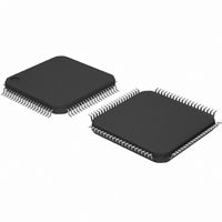
PCF8534AH/1,518 NXP Semiconductors, PCF8534AH/1,518 Datasheet - Page 15

PCF8534AH/1,518
Manufacturer Part Number
PCF8534AH/1,518
Description
IC LCD DVR UNVRSL LOW-MUX 80LQFP
Manufacturer
NXP Semiconductors
Datasheet
1.PCF8534AH1518.pdf
(44 pages)
Specifications of PCF8534AH/1,518
Package / Case
80-LQFP
Display Type
LCD
Configuration
60 Segment
Interface
I²C
Current - Supply
8µA
Voltage - Supply
1.8 V ~ 5.5 V
Operating Temperature
-40°C ~ 85°C
Mounting Type
Surface Mount
Number Of Digits
30
Number Of Segments
240
Maximum Clock Frequency
400 KHz
Operating Supply Voltage
1.8 V to 5.5 V
Maximum Power Dissipation
400 mW
Maximum Operating Temperature
+ 85 C
Maximum Supply Current
50 mA
Minimum Operating Temperature
- 40 C
Lead Free Status / RoHS Status
Lead free / RoHS Compliant
Digits Or Characters
-
Lead Free Status / Rohs Status
Details
Other names
935284829518
PCF8534AH/1-T
PCF8534AH/1-T
PCF8534AH/1-T
PCF8534AH/1-T
Available stocks
Company
Part Number
Manufacturer
Quantity
Price
Company:
Part Number:
PCF8534AH/1,518
Manufacturer:
NXP Semiconductors
Quantity:
10 000
Part Number:
PCF8534AH/1,518
Manufacturer:
NXP/恩智浦
Quantity:
20 000
NXP Semiconductors
PCF8534A_3
Product data sheet
7.11 Data pointer
The following applies to
The addressing mechanism for the display RAM is realized using the data pointer. This
allows the loading of an individual display data byte or a series of display data bytes, into
any location of the display RAM. The sequence commences with the initialization of the
data pointer by the load data pointer command. After this, the data byte is stored starting
at the display RAM address indicated by the data pointer (see
is stored, the data pointer is automatically incremented based on the selected LCD
configuration.
The contents of the data pointer are incremented as follows:
If an I
Consequently, the data pointer must be rewritten prior to further RAM accesses.
•
•
•
•
•
•
•
•
Static drive mode: the eight transmitted data bits are placed in row 0 to eight
successive display RAM addresses.
1:2 multiplex drive mode: the eight transmitted data bits are placed in row 0 and 1 to
four successive display RAM addresses.
1:3 multiplex drive mode: the eight transmitted data bits are placed in row 0, 1 and 2
to three successive addresses. However, bit 2 of the third address is left unchanged.
This last bit can, if necessary, be controlled by an additional transfer to this address
but avoid overriding adjacent data because full bytes are always transmitted.
1:4 multiplex drive mode: the eight transmitted data bits are placed in
row 0, 1, 2 and 3 to two successive display RAM addresses.
In static drive mode by eight.
In 1:2 multiplex drive mode by four.
In 1:3 multiplex drive mode by three.
In 1:4 multiplex drive mode by two.
2
C-bus data access terminates early, the state of the data pointer is unknown.
Rev. 03 — 10 November 2008
Figure
11:
Universal LCD driver for low multiplex rates
Figure
PCF8534A
11). Once each byte
© NXP B.V. 2008. All rights reserved.
15 of 44


