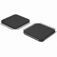
PCF8534AH/1,518 NXP Semiconductors, PCF8534AH/1,518 Datasheet - Page 14

PCF8534AH/1,518
Manufacturer Part Number
PCF8534AH/1,518
Description
IC LCD DVR UNVRSL LOW-MUX 80LQFP
Manufacturer
NXP Semiconductors
Datasheet
1.PCF8534AH1518.pdf
(44 pages)
Specifications of PCF8534AH/1,518
Package / Case
80-LQFP
Display Type
LCD
Configuration
60 Segment
Interface
I²C
Current - Supply
8µA
Voltage - Supply
1.8 V ~ 5.5 V
Operating Temperature
-40°C ~ 85°C
Mounting Type
Surface Mount
Number Of Digits
30
Number Of Segments
240
Maximum Clock Frequency
400 KHz
Operating Supply Voltage
1.8 V to 5.5 V
Maximum Power Dissipation
400 mW
Maximum Operating Temperature
+ 85 C
Maximum Supply Current
50 mA
Minimum Operating Temperature
- 40 C
Lead Free Status / RoHS Status
Lead free / RoHS Compliant
Digits Or Characters
-
Lead Free Status / Rohs Status
Details
Other names
935284829518
PCF8534AH/1-T
PCF8534AH/1-T
PCF8534AH/1-T
PCF8534AH/1-T
Available stocks
Company
Part Number
Manufacturer
Quantity
Price
Company:
Part Number:
PCF8534AH/1,518
Manufacturer:
NXP Semiconductors
Quantity:
10 000
Part Number:
PCF8534AH/1,518
Manufacturer:
NXP/恩智浦
Quantity:
20 000
NXP Semiconductors
PCF8534A_3
Product data sheet
7.10 Display RAM
7.9 Backplane outputs
The LCD drive section includes four backplane outputs: BP0 to BP3. The backplane
output signals are generated based on the selected LCD drive mode.
If less than four backplane outputs are required the unused outputs can be left as an
open-circuit.
The display RAM is static 60
map indicates the on-state of the corresponding LCD segment, logic 0 indicates the
off-state. There is a direct relationship between RAM addresses and the segment outputs
and the individual bits of a RAM word and the backplane outputs. The first RAM row
corresponds to the 60 segments operated with respect to backplane BP0 (see
In multiplexed LCD applications, the segment data of rows 1 to 4 of the display RAM are
time-multiplexed with BP0, BP1, BP2 and BP3, respectively.
When display data is transmitted to the PCF8534A, the display bytes received are stored
in the display RAM based on the selected LCD drive mode. Data is stored as it arrives and
does not wait for the acknowledge cycle. Depending on the current multiplexer mode data
is stored singularly, in pairs, triplets or quadruplets. In 1:2 multiplexer mode for example,
RAM data is stored every second bit. An example of a 7-segment numeric display
illustrating the storage order for all drive modes is shown in
organization applies equally to other LCD types.
Fig 10. Display RAM bit map
•
•
•
•
In 1:4 multiplex drive mode: BP0 to BP3 must be connected directly to the LCD.
In 1:3 multiplex drive mode: BP3 carries the same signal as BP1, therefore these two
adjacent outputs can be tied together to give enhanced drive capabilities.
In 1:2 multiplex drive mode: BP0 and BP2, BP1 and BP3 respectively carry the same
signals and can also be paired to increase the drive capabilities.
In static drive mode: the same signal is carried by all four backplane outputs and they
can be connected in parallel for very high drive requirements.
backplane outputs
display RAM bits
Display RAM bit map showing the direct relationship between backplane outputs, display RAM
addresses and segment outputs and between bits in a RAM word and backplane outputs.
(rows)/
(BP)
Rev. 03 — 10 November 2008
0
1
2
3
0
1
4-bit RAM which stores LCD data. Logic 1 in the RAM bit
2
display RAM addresses (columns)/segment outputs (S)
3
4
Universal LCD driver for low multiplex rates
Figure
55
11. The RAM storage
PCF8534A
56
© NXP B.V. 2008. All rights reserved.
57
001aah617
58
Figure
59
14 of 44
10).


